Reference sheet
Decoupling capacitors
Why every IC needs one, which values, and where to put them
Decoupling capacitor guide
Digital ICs don't draw a steady current — their internal gates switch in nanoseconds, pulling short, sharp current spikes from the supply pin. The trace back to the regulator has inductance and can't react that fast, so without help the local supply voltage dips or rings every time the chip switches. A decoupling (or bypass) capacitor sits right at the pin as a tiny local charge reservoir: it supplies that fast current itself, so the regulator only has to deal with the slower average load.
The usual arrangement is two tiers. A small ceramic, almost always around 100 nF, sits directly on the IC's supply pin and handles the fast, high-frequency transients. A larger bulk capacitor, typically in the 1-10 µF range, feeds a small group of nearby ICs or a section of a power rail and restocks the charge those small caps used up, responding to slower, lower-frequency current swings.
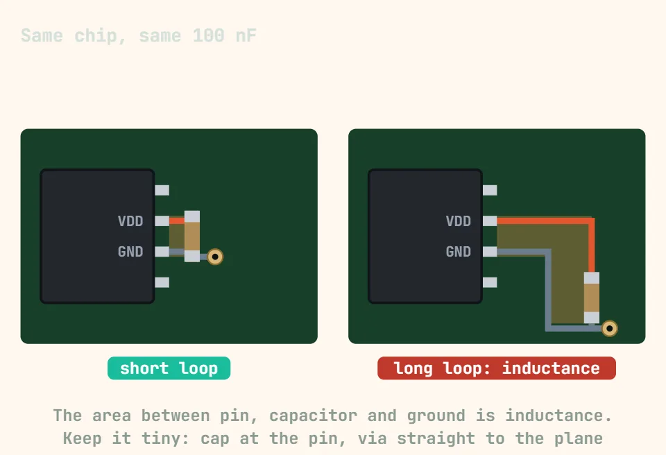
Placement matters as much as the printed value. Every millimeter of trace or via between the capacitor and the pin adds parasitic inductance, and that inductance — not the capacitor's rated capacitance — is usually what limits how well it can respond at the frequencies decoupling is meant to fix. The rule of thumb: put it as close to the pin as the footprint allows, with the shortest possible path, ideally a dedicated via straight down, to the ground plane.
| Situation / topic | Typical value(s) | Placement | Why it matters |
|---|---|---|---|
| Standard logic IC / gate (e.g. 74xx, simple CMOS) | 100 nF (0.1 µF) ceramic, X7R | Directly across the supply pin, shortest possible trace and via to the ground plane | The default bypass cap for almost any digital IC; handles fast switching transients |
| Microcontroller VDD pin(s) | 100 nF ceramic per VDD pin | One capacitor per physical VDD pin, right at that pin — not shared between pins | Parts with several VDD pins usually need one cap per pin; follow the datasheet's own decoupling diagram rather than assuming |
| MCU/SoC core rail (separate from I/O supply) | 100 nF, sometimes plus 1 µF — value varies by part, check the datasheet | At the dedicated core-supply pin, as close as the package allows | Core logic rails are often noisier and lower-voltage than I/O rails; manufacturers usually specify an exact decoupling network, so don't guess |
| RF module (BLE / Wi-Fi / LoRa) supply pin | 100 nF, sometimes with a smaller-value cap (a few nF) added alongside | Tight to the pin, routed clear of the antenna keepout area | RF front ends are sensitive to supply noise; follow the module's reference layout rather than improvising |
| Bulk/reservoir cap for a small group of ICs | 1-10 µF ceramic (X5R/X7R) or tantalum | One per every few ICs, or where power enters a section of the board | Restocks the charge the small 100 nF caps used up; responds to slower current swings than pin-level caps do |
| Bulk cap at a regulator's output | 10-100 µF — electrolytic, polymer, or large ceramic depending on the regulator | Immediately at the regulator's output pin | Also part of the regulator's stability/compensation network — use the value, type and ESR range the regulator's datasheet specifies, don't substitute freely |
| Analog IC / op-amp supply pin | 100 nF ceramic close to the pin, sometimes with a 1-10 µF bulk cap nearby | Right at the pin; keep analog and digital decoupling/ground separate where the design has both | Analog stages are more sensitive to supply noise coupling in than plain digital logic |
| High pin-count part (FPGA, SoC, dense BGA) | Many caps of mixed values (e.g. 100 nF and 1 µF, sometimes smaller values too) | One capacitor per power-pin escape via, spread under the footprint rather than clustered on one side | A single value can't cover the wide frequency range these parts demand; follow the vendor's power-delivery/decoupling app note |
| When to use two values in parallel | e.g. 100 nF + 1 µF, or 100 nF + 10 µF | Smaller value closest to the pin, larger value can sit slightly farther out | Widens the frequency range of low impedance; space the values roughly a decade apart so their parallel-resonance peak stays small and away from where it matters |
| Ceramic dielectric choice | X7R for general-purpose decoupling; C0G/NP0 for precision analog/RF; avoid Y5V/Z5U for decoupling | Same placement rules apply regardless of dielectric | X7R stays reasonably stable with voltage and temperature; Y5V/Z5U capacitance can collapse under bias — fine for some filtering, poor for a supply pin |
| Trace/via geometry | Applies to any decoupling cap, not a specific value | Shortest possible pad-to-via run; via drops straight to the ground-plane layer rather than routing sideways first | Loop inductance from the mounting geometry often matters more than the capacitor's own rated value at these frequencies |
| Package size (0402, 0603, 0805…) | 0402 or smaller preferred for high-speed decoupling where assembly allows; 0603/0805 common on hobby or hand-assembled boards | Same as any decoupling cap — as close to the pin as the footprint allows | Smaller packages have lower parasitic inductance (ESL) for the same capacitance, which matters more as switching speeds rise |
A cap's printed value is a starting point, not gospel: small ceramics lose a real chunk of their rated capacitance once DC bias and temperature are applied, so check the manufacturer's DC-bias derating curve rather than the datasheet's nominal number on a marginal design. And more capacitors isn't automatically better — stacking values that are too close together (or too far apart with nothing in between) can create a parallel resonance where the combined impedance briefly rises instead of falling; a roughly decade-spaced pair (100 nF + 1 µF, not 100 nF + 100 µF right next to it) avoids that trap.