Pinout
SWD debug (2-wire, ARM Cortex-M) pinout
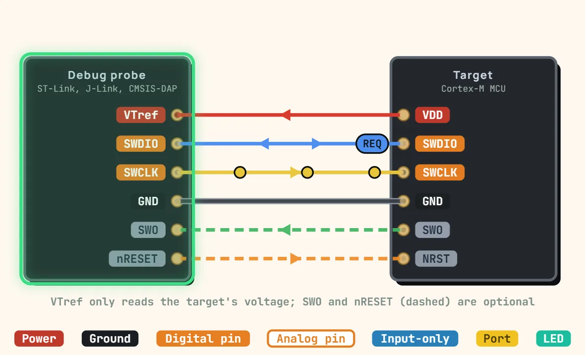
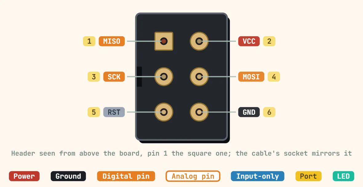
Pins
- VCC (target reference voltage)
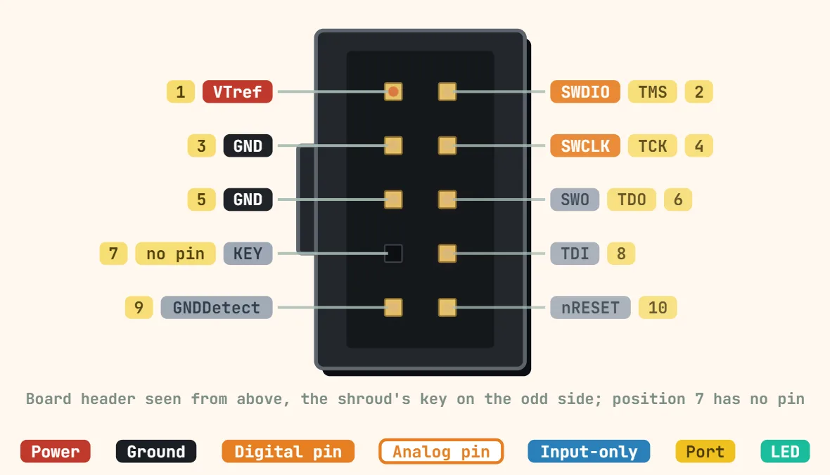
- SWDIO (bidirectional data)
- SWCLK (clock)
- GND
- Optional: RESET and SWO (trace) on some debuggers
Specifications
| Signals | SWDIO, SWCLK + GND, VTref |
|---|---|
| Optional | nRESET, SWO trace |
| Topology | Point-to-point (one probe, one target) |
| Duplex | Half duplex (SWDIO bidirectional) |
| Logic level | Target I/O voltage, sensed on VTref |
| Pull resistors | SWDIO pull-up, SWCLK pull-down (often internal) |
| SWO trace | Cortex-M3 and above, not M0 / M0+ |
| STM32 pins | PA13 (SWDIO), PA14 (SWCLK) |
| Standard connector | 10-pin 1.27 mm Cortex Debug |
| Typical probes | ST-Link, J-Link, CMSIS-DAP, Picoprobe |
Notes
- Two signals do everything: SWCLK, driven by the probe, and SWDIO, which changes direction during each transfer. GND is mandatory. VTref is an INPUT of the probe: it reads the target's I/O voltage to set its own logic levels and does not power the board.
- The small ST-Link clone dongles are the exception: their 3.3V and 5V pins are real supply outputs and can power a small target — never while the target also has its own supply connected.
- nRESET is optional for ordinary flashing, but it lets the probe connect under reset when the firmware has reconfigured the debug pins or sleeps too deeply to answer. SWO is a one-way trace output (printf-style ITM data); Cortex-M0 and M0+ cores do not have it.
- On an STM32 the pins are PA13 (SWDIO) and PA14 (SWCLK): firmware that reuses them as ordinary GPIO locks the probe out until the next connect under reset. A Raspberry Pi Pico brings its dedicated SWD pins out on the three DEBUG pads.