Pinout
ARM Cortex Debug connector (10-pin, 1.27mm) pinout
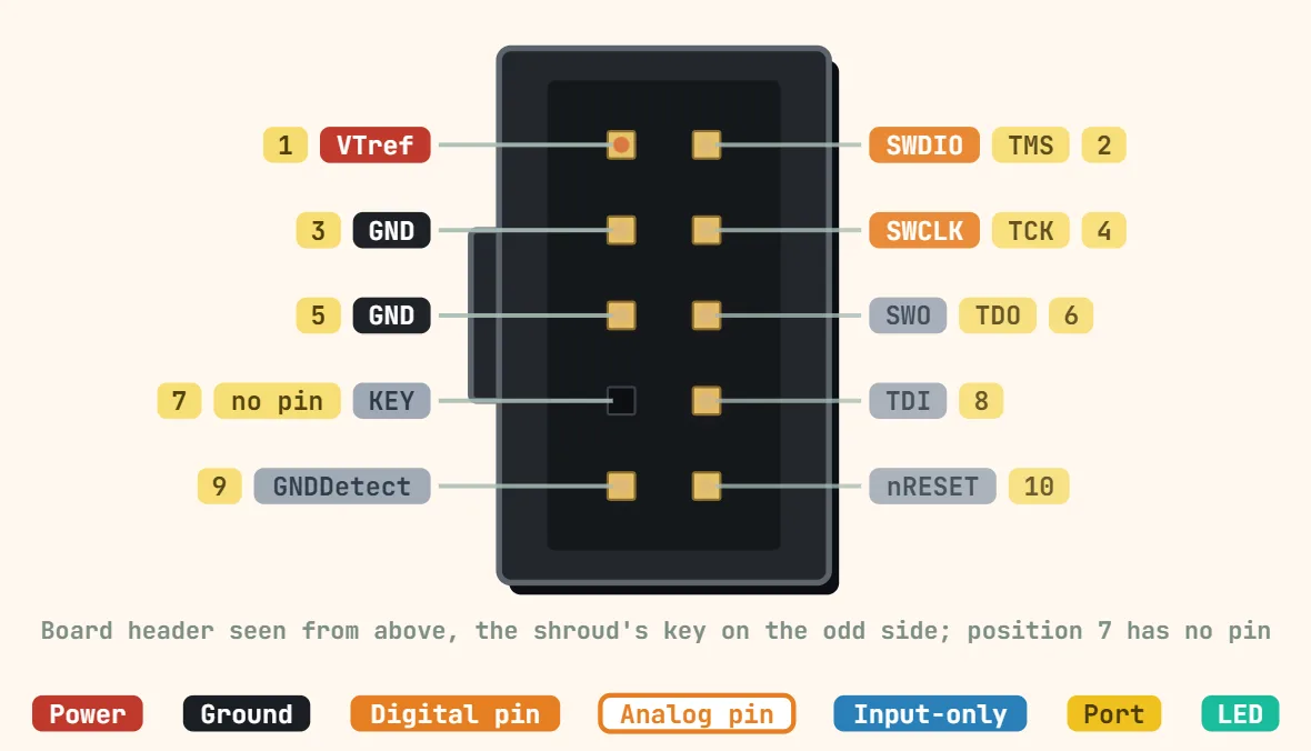
Pins
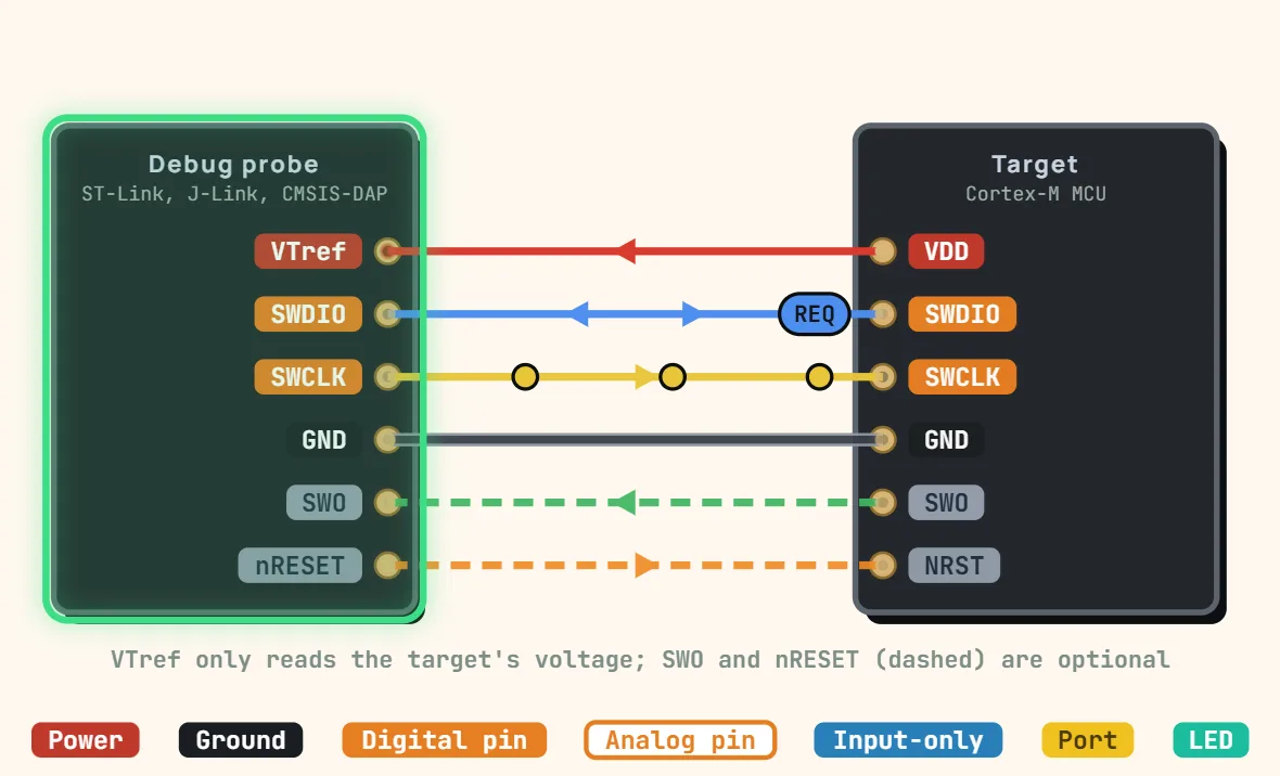
- 1: VTref (probe INPUT — tells the debugger the target's I/O voltage; never used to power the target)
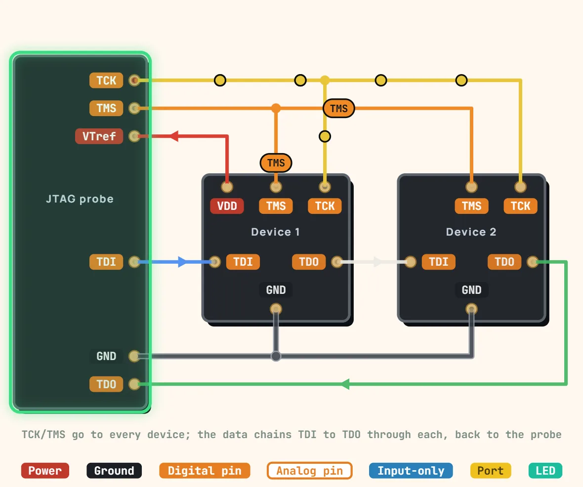
- 2: SWDIO / TMS (bidirectional data — also the JTAG mode-select line)
- 3: GND
- 4: SWCLK / TCK (clock — also the JTAG clock)
- 5: GND
- 6: SWO / TDO (trace output)
- 7: KEY — no physical pin here by design; this is a blocked hole, not a signal
- 8: NC / TDI (reserved for full-JTAG mode; unused in SWD-only debugging)
- 9: GNDDetect
- 10: nRESET
Specifications
| Contacts | 10 (2 × 5), pin 7 removed as key |
|---|---|
| Pitch | 1.27 mm |
| Protocols | SWD, JTAG, SWO trace |
| Minimum for SWD | VTref, SWDIO, SWCLK, GND |
| VTref | Probe input, never powers the target |
| Logic level | Target I/O voltage |
| Typical header | Samtec FTSH-105 (shrouded, keyed) |
| Cable | 10-way 1.27 mm ribbon |
| Older alternative | 20-pin 2.54 mm ARM JTAG header |
Notes
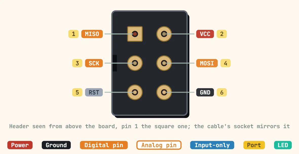
- The drawing is the header on the board seen from above. On a shrouded header the key notch is on the odd-pin side (1, 3, 5, 7, 9); on a bare header, look for the pin-1 mark on the silkscreen.
- The official ARM CoreSight standard (the small 2×5, 1.27mm-pitch header nearly every modern Cortex-M board carries) — not the older, larger 20-pin/0.1" ARM JTAG header, which is a different connector with a different pin count and numbering.
- Pin 7's missing pin is the mechanical key: it is what lets a shrouded 2×5 header only insert one way. Do not mistake it for a spare signal pin when laying out a mating connector.
- SWD-only debugging needs just VTref, SWDIO, SWCLK and GND — SWO and nRESET are worth wiring if the debugger and target both support them, but are not required for basic flash/step.
- This is what the app's own SWD entry above is meant to connect through — the SWD signals are the same two wires either way, this is just the standardized connector they land on.