Pinout
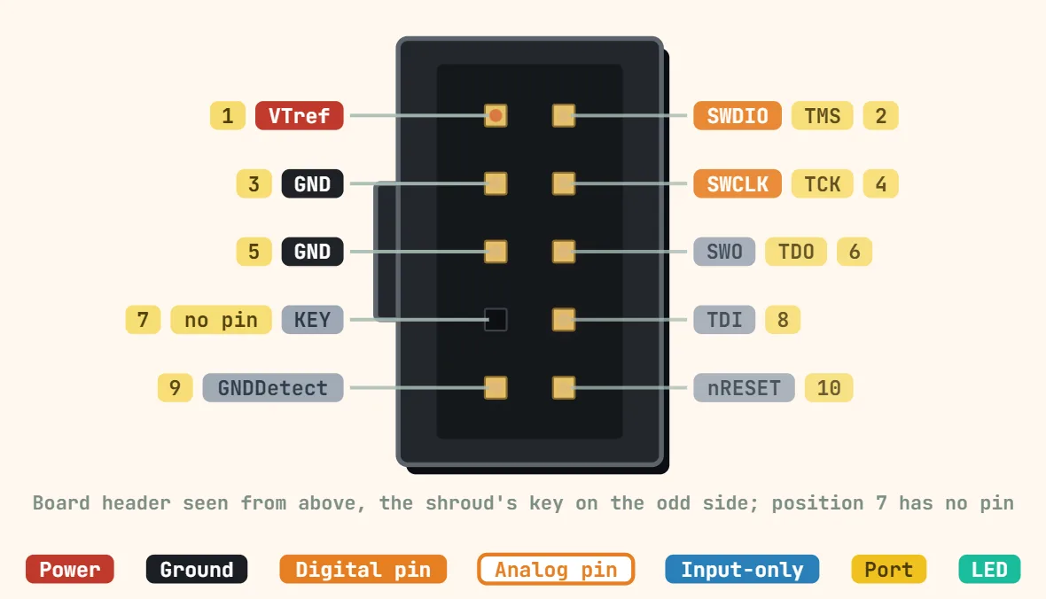
JTAG (4-wire debug, common subset) pinout
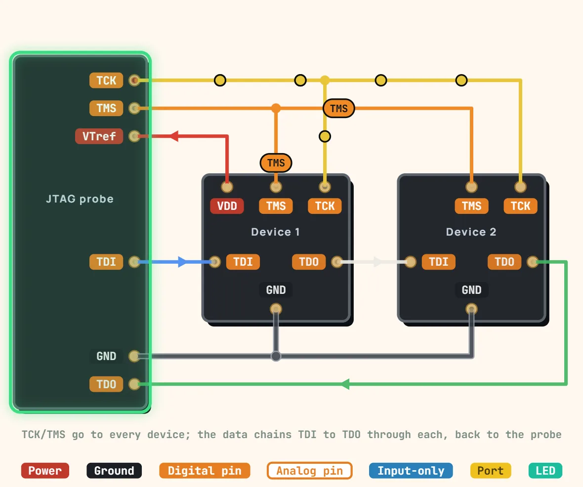
Pins
- TDI (data in)
- TDO (data out)
- TCK (clock)
- TMS (mode select)
- Often paired with VCC, GND, and nRESET on the connector
Specifications
| Standard | IEEE 1149.1 |
|---|---|
| Signals | TCK, TMS, TDI, TDO (+ optional TRST) |
| Topology | Daisy chain on TDI → TDO, TCK / TMS shared |
| Clock edges | TMS / TDI sampled on rising TCK, TDO changes on falling |
| Logic level | Target I/O voltage, sensed on VTref |
| Pull-ups | TMS and TDI held high when undriven |
| Common connectors | 20-pin 2.54 mm (ARM), 10-pin 1.27 mm Cortex Debug |
| Uses | Debug, flash programming, boundary scan |
| JTAG-only targets | FPGAs, CPLDs, ESP32 |
Notes
- TCK and TMS go to every device in parallel; the data forms a chain — the probe's TDI into the first device, each TDO into the next TDI, the last TDO back to the probe. A board with a single chip is simply a chain of one.
- TMS and TDI are sampled on the rising edge of TCK and TDO changes on the falling edge. Besides the four signals a probe needs GND and usually VTref (the target's I/O voltage, a sense input); the nTRST and nSRST reset lines are optional.
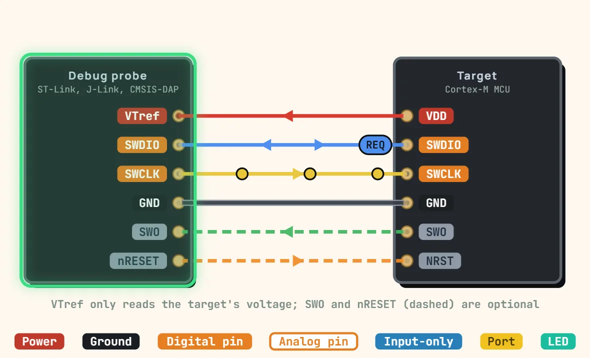
- On ARM Cortex parts the same pins double as SWD — TMS is SWDIO and TCK is SWCLK — which is why the small 10-pin Cortex Debug connector carries both. FPGAs, CPLDs and the ESP32 family are JTAG-only.