Pinout
ESP8266 NodeMCU pinout
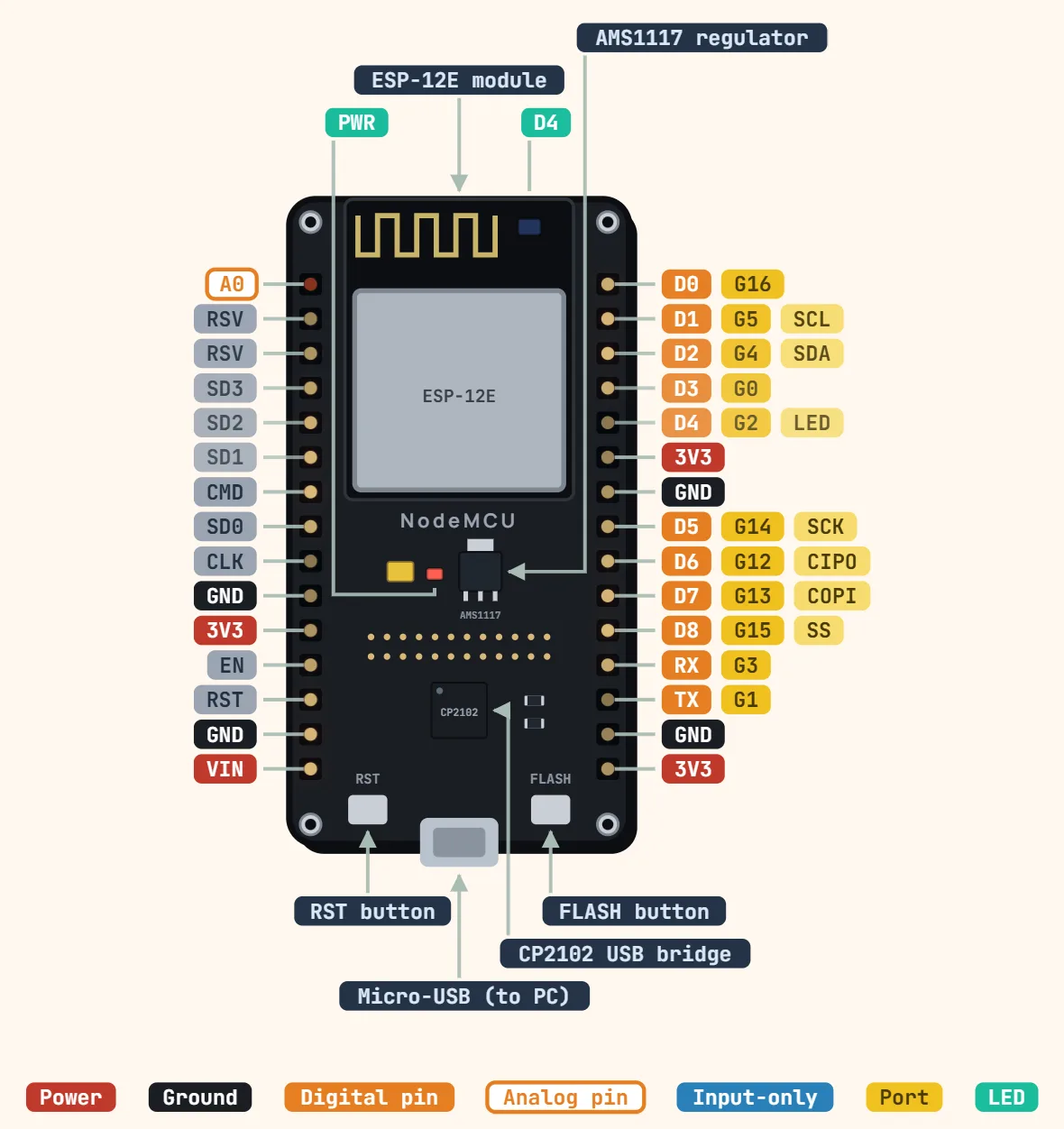
Pins
- A0
- RSV
- RSV
- SD3
- SD2
- SD1
- CMD
- SD0
- CLK
- GND
- 3V3
- EN
- RST
- GND
- VIN
- D0 — G16
- D1 — G5 — SCL
- D2 — G4 — SDA
- D3 — G0
- D4 — G2 — LED
- 3V3
- GND
- D5 — G14 — SCK
- D6 — G12 — CIPO
- D7 — G13 — COPI
- D8 — G15 — SS
- RX — G3
- TX — G1
- GND
- 3V3
Specifications
| Module | ESP-12E/ESP-12F (ESP8266EX) |
|---|---|
| CPU | Tensilica L106, 80 MHz (160 MHz option) |
| Flash memory | 4 MB |
| Supply | 5 V via USB or VIN, onboard 3.3 V regulator |
| Logic level | 3.3 V |
| GPIO current | 12 mA max per pin |
| Digital I/O | D0–D8 plus RX/TX (D0 has no PWM or interrupt) |
| Analog input | 1 × 10-bit (A0, 0–3.3 V via onboard divider) |
| Wi-Fi | 802.11 b/g/n, 2.4 GHz |
| USB | Micro-USB, CP2102 (v1.0) or CH340G (v3) |
Boot & strapping
- GPIO0 (D3): LOW at reset drops the chip into UART flashing mode; HIGH — the default, usually via an onboard pull-up — boots the sketch normally.
- GPIO2 (D4, also the onboard blue LED on most boards): must be HIGH at reset. Conveniently, that is also the LED’s off state, so wiring the LED there doesn’t fight the strap.
- GPIO15 (D8): must be LOW at reset for either boot path to succeed — this board usually ships with a pull-down already in place. A pull-up wired here, or an SPI device that idles its chip-select pin HIGH, can be enough to stop the board booting.
- Most NodeMCU boards wire their USB-serial chip’s DTR/RTS lines to toggle GPIO0 and RST automatically during upload, so flashing normally needs no button press — on a board without that circuit, hold FLASH (GPIO0 low) while tapping RST, then release FLASH once the upload starts.
Notes
- A0 has an onboard voltage divider so it reads 0–3.3V — the bare ESP8266 chip’s own ADC input only accepts 0–1.0V, so a design written against the raw chip’s spec does not carry over to this board unmodified.
- D0 (GPIO16) is the odd one out: no PWM, no interrupt support, and it is the pin wired to RST to wake the chip from deep sleep — that wire is what makes deep sleep work at all on this board.
- The silkscreened "D" numbers (D0–D8) are this board’s own numbering layer, not the underlying GPIO numbers: D0 is GPIO16, D1 is GPIO5, D3 is GPIO0, and so on — a library or tutorial written against "GPIO0" means D3 here, not D0.
- ADC readings can get noisy during an active Wi-Fi transmission burst — the single ADC shares board space with the radio. A small filter capacitor on A0, or averaging a few readings, is the usual fix; unlike the ESP32, there is no second ADC to switch to.
- Each GPIO is rated for a maximum of 12mA — noticeably less headroom than an AVR board’s 40mA, so driving even a single LED without its own series resistor is closer to the pin’s actual limit here. The same Wi-Fi-transmit-burst-vs-onboard-regulator caution as the ESP32 DevKit above applies: a marginal USB supply plus a transmit peak is the classic cause of a random reset that looks like a code bug.