Pinout
ESP-01 (ESP8266, 2×4 header) pinout
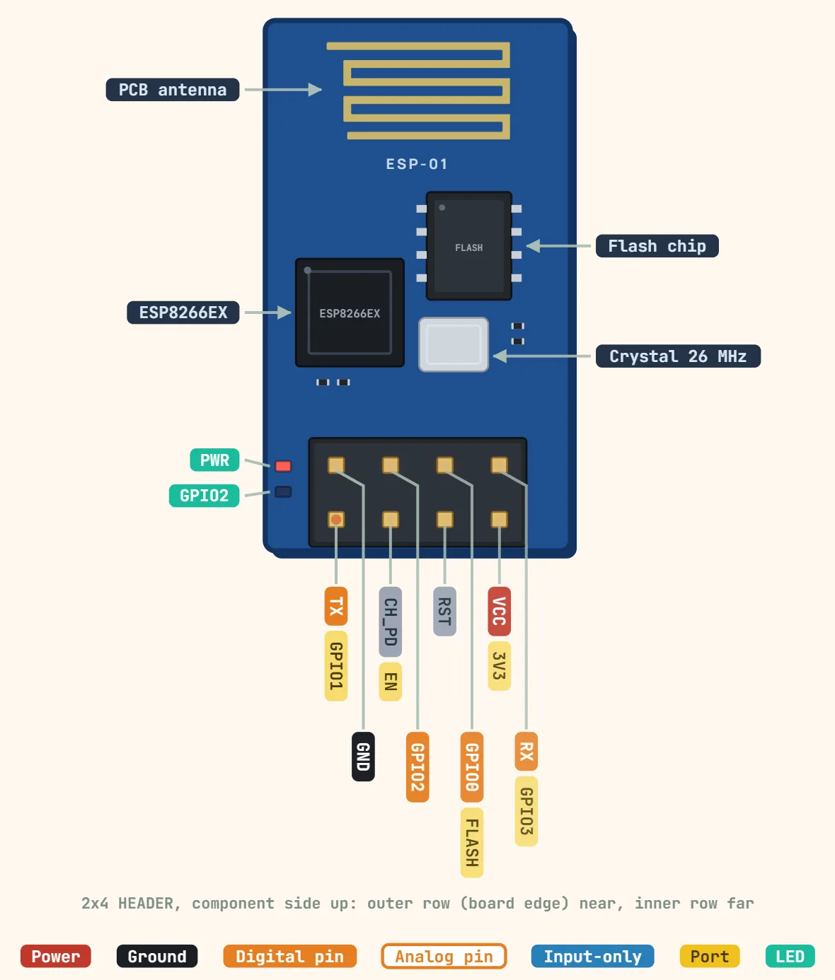
Pins
- Outer row (board edge): TX — GPIO1
- Outer row (board edge): CH_PD — EN
- Outer row (board edge): RST
- Outer row (board edge): VCC — 3V3
- Inner row: GND
- Inner row: GPIO2
- Inner row: GPIO0 — FLASH
- Inner row: RX — GPIO3
Specifications
| Chip | ESP8266EX |
|---|---|
| CPU | Tensilica L106, 80 MHz (160 MHz option) |
| Flash memory | 512 KB (ESP-01) or 1 MB (ESP-01S) |
| Supply voltage | 3.3 V (3.0–3.6 V) |
| Logic level | 3.3 V (not 5 V tolerant) |
| Peak current | ≈ 170 mA during Wi-Fi transmit (plan for 300 mA) |
| GPIO current | 12 mA max per pin |
| Usable GPIO | GPIO0, GPIO2 (+ GPIO1/3 if serial unused) |
| Wi-Fi | 802.11 b/g/n, 2.4 GHz |
| Interface | UART (AT firmware or custom sketch) |
| Size | 24.8 × 14.3 mm |
Notes
- Eight pins on a 2×4 male header at one end, read from the component side with the antenna pointing away: the row along the board edge is TX, CH_PD, RST, VCC; the inner row is GND, GPIO2, GPIO0, RX. Two rows at 0.1" means it will not plug into a breadboard without shorting the rows — use an adapter board or jumper wires.
- 3.3V ONLY, on VCC and on every signal pin: nothing on this module is 5V tolerant. A USB-TTL adapter’s own 3.3V pin usually cannot supply the 200–300mA bursts Wi-Fi draws, which shows up as random resets — give it a proper 3.3V regulator.
- CH_PD (EN) must be tied HIGH for the chip to run at all, and RST is active-low. GPIO0 LOW at reset enters UART flash mode, HIGH boots the sketch; GPIO2 must be HIGH at reset — so neither strapping pin can be used as an input that might be low at power-up.
- Only GPIO0 and GPIO2 are spare I/O; TX and RX (GPIO1/GPIO3) can be repurposed as GPIO once serial is no longer needed, at the cost of the serial monitor.