Pinout
ESP32 pinout (DevKit V1, 30-pin)
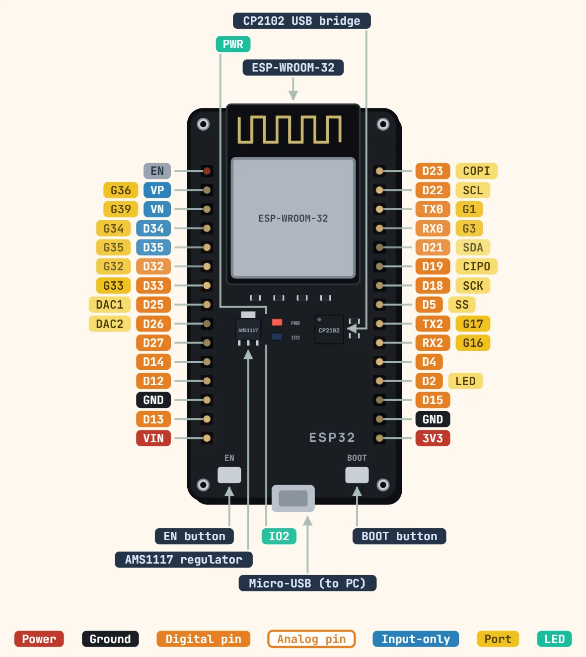
Pins
- EN
- VP — G36
- VN — G39
- D34 — G34
- D35 — G35
- D32 — G32
- D33 — G33
- D25 — DAC1
- D26 — DAC2
- D27
- D14
- D12
- GND
- D13
- VIN
- D23 — COPI
- D22 — SCL
- TX0 — G1
- RX0 — G3
- D21 — SDA
- D19 — CIPO
- D18 — SCK
- D5 — SS
- TX2 — G17
- RX2 — G16
- D4
- D2 — LED
- D15
- GND
- 3V3
Specifications
| Module | ESP32-WROOM-32 |
|---|---|
| CPU | Dual-core Xtensa LX6, up to 240 MHz |
| SRAM | 520 KB |
| Flash memory | 4 MB (external SPI) |
| Supply | 5 V via USB or VIN, onboard 3.3 V regulator |
| Logic level | 3.3 V (not 5 V tolerant) |
| GPIO on header | 25 (GPIO34–39 input-only) |
| GPIO current | 40 mA source / 28 mA sink max per pin |
| ADC | 12-bit SAR; ADC1 usable with Wi-Fi, ADC2 not |
| DAC | 2 × 8-bit (GPIO25, GPIO26) |
| Wi-Fi | 802.11 b/g/n, 2.4 GHz |
| Bluetooth | v4.2 Classic + BLE |
| USB | Micro-USB, CP2102 or CH340 USB-serial (varies by clone) |
Boot & strapping
- GPIO12 (D12) is the one that actually bricks a boot: it selects the flash chip’s own supply voltage, and pulled HIGH at reset it switches that rail to 1.8V — a standard 3.3V flash chip can’t be read at that voltage, so the board never starts. Leave anything wired to D12 free to float or read low at power-up.
- GPIO15 (D15) only controls whether the ROM bootloader prints its startup log over the USB serial port — LOW at reset silences that log, nothing more. If a wire on D15 seems to stop the board, check the serial monitor before assuming a real fault.
- GPIO0, the pin behind the onboard BOOT button, isn’t broken out to a header pin on this 30-pin layout at all. Holding BOOT while tapping EN pulls both GPIO0 and GPIO2 low together, which is what actually drops the chip into flashing mode.
- GPIO2 (D2, also the onboard LED on most boards) only matters jointly with GPIO0 during that flash-mode entry — it plays no part in a normal boot, so wiring an LED there (its usual job) is safe.
- GPIO5 (D5) is technically a fifth strapping pin, but it only sets an SDIO-slave clock-timing option this board never uses in a normal Arduino/ESP-IDF sketch — of the five, it is the one least likely to ever cause a real problem.
Notes
- GPIO6–11 connect to the module’s own SPI flash and are not broken out to header pins on this 30-pin layout — if a diagram shows them, it is a different (usually 38-pin) board, not this one.
- Logic is 3.3V only. VIN/5V feeds the onboard regulator down to 3.3V; the ESP32 die itself is not 5V tolerant on any GPIO.
- GPIO34, GPIO35, GPIO36 (VP) and GPIO39 (VN) are input-only — no output driver and no internal pull-up/pull-down, so an unconnected one floats and needs its own external resistor.
- ADC2 covers GPIO0, 2, 4, 12, 13, 14, 15, 25, 26 and 27 — all ten stop giving usable readings the moment Wi-Fi is active, since the radio and ADC2 share hardware. Need an analog reading alongside Wi-Fi? Use an ADC1 pin instead — on this board, that’s VP/VN/D34/D35/D32/D33.
- There is no standard "pin 1 to 30" numbering for this board: generic clones disagree on layout, and every reference — including this board’s own silkscreen — only ever names pins by GPIO number.
- EN is the active-low reset pin — briefly tie it to GND to reset the chip in circuit, the same role RESET plays on an AVR board.
- The onboard regulator stepping VIN/5V down to 3.3V is usually rated for several hundred mA at most (commonly an AMS1117 or similar on this class of board — check yours), while the ESP32 itself can pull momentary current peaks of a few hundred mA during a Wi-Fi transmit burst. A weak USB cable/port plus a marginal regulator is the classic cause of a board that randomly resets specifically when Wi-Fi is active, not at any other time — a symptom that looks like a code bug but is really a power problem.