Reference sheet
PCB stackup
2, 4 or 6 layers, and what a ground plane buys you
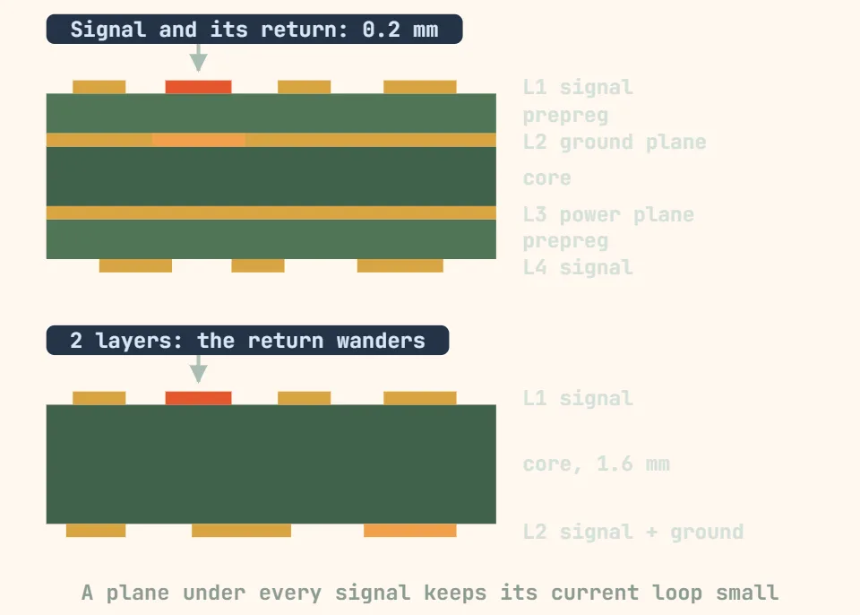
PCB stackup & layer count guide
Layer count is really a routing-density and signal-integrity decision, not a fixed rule. A simple board with a handful of parts and slow signals routes fine on 2 layers; once you have a microcontroller with dozens of pins, multiple power rails, or anything running faster than a few tens of MHz, a 4-layer board is the usual default because it adds a dedicated ground plane without a big cost jump. Push past that only when routing congestion, EMI limits, or high-speed interfaces (USB3, HDMI, DDR, PCIe) force it.
A dedicated ground (or power) plane is a full sheet of copper, not a trace, and that is what makes it useful. High-frequency return current takes the path of least impedance, which is the plane area directly beneath the signal trace, so the outgoing and returning current form a tight loop with almost no extra area. That small loop area is what actually lowers radiated EMI and crosstalk, and it also gives every trace a constant, predictable reference for controlled-impedance routing - something you cannot get reliably on a 2-layer board with no full plane.
A common 4-layer order is Signal / GND / PWR / Signal (top to bottom). Both outer signal layers sit directly next to a plane, which keeps their reference distance short and their impedance predictable, and stacking GND next to PWR turns the thin dielectric between them into a broad, low-inductance decoupling capacitor that helps stabilize the power rail. Some fabs and designers swap to Signal / GND / Signal / PWR instead, trading a bit of power-plane quality for a better-referenced inner routing layer - ask your fab which they optimize for.
Every extra layer pair adds lamination cycles, drilling, and material, so cost rises with layer count, and boards are almost always specified in even numbers (2, 4, 6, 8...) because fabs build them as symmetric stacks to avoid warping during lamination - odd counts like 3 or 5 are non-standard and usually cost more, not less. The practical approach is to pick the fewest layers that meet your routing density, EMI, and signal-integrity needs, since exact price ratios between layer counts vary a lot by manufacturer, quantity, and turn time.
| Layers | Typical stackup (top → bottom) | Typical use case | Relative cost | When to choose it |
|---|---|---|---|---|
| 1 (single-sided) | Signal only, bare substrate on the other side | Very simple hobby boards, LED boards, basic power adapters | Lowest | Trivial routing, extreme cost sensitivity, no real speed or EMI concerns |
| 2 (double-sided) | Signal (top) / Signal (bottom), no dedicated plane | Maker/hobbyist boards, simple MCU projects, basic analog circuits | Low - the usual baseline | Low pin count, slow signals (roughly sub-10-30 MHz), tight budget, EMI not a hard requirement |
| 4 - GND/PWR sandwich | Signal / GND / PWR / Signal | Most commercial embedded products: MCU boards, sensor boards, USB2, I2C/SPI/general digital | Moderate (varies by fab, often ~1.5-3x a 2-layer board) | Default for real products - clean return path, decent EMI control, still routable by hand or auto-router |
| 4 - alt order | Signal / GND / Signal / PWR | Same class of product as above, when the inner layer needs to carry more traces | Similar to the sandwich order | Need extra inner routing capacity and can trade a slightly noisier power plane for it |
| 6 | Signal / GND / Signal / Signal / PWR / Signal (varies by fab) | Denser boards: multiple MCUs, several power rails, moderate-speed digital, more shielding between signal layers | Higher than 4-layer (roughly 2-4x, fab-dependent) | 4-layer routing is too congested, or you need extra plane isolation between noisy and sensitive signal layers |
| 8 | Multiple signal/plane pairs, often with blind or buried vias | Dense BGA breakout, PCIe/USB3/HDMI/Gigabit Ethernet, several independent voltage domains | Significantly higher; may require microvia/blind-via processes | High pin-count BGAs, strict impedance/signal-integrity targets, each rail needs its own plane |
| 10+ | Multiple dedicated signal, ground, and power planes, advanced via structures | High-speed SoC/FPGA boards, RF/microwave modules, dense networking or server boards | Highest; longer lead times, tighter fab tolerances | DDR4/5 or PCIe Gen4+ class interfaces, RF stripline layers, extreme routing density |
Get an exact stackup and impedance calc from your fab before finalizing a design - dielectric thickness, copper weight, and layer order all shift the numbers, and two manufacturers' "4-layer standard stackup" are rarely identical.