Reference sheet
PCB design rules
Trace width and current, spacing, rings, drills, copper weight
PCB design rules
Trace widths from the IPC-2221 curve fit, I = 0.048 × ΔT^0.44 × A^0.725 on outer layers, with A the cross-section in mil² and half the constant on inner layers. ΔT is how much hotter than ambient you will let the copper run: 10 °C is the normal budget, 20 °C is defensible for a short run to a connector. Inner layers carry about half, because there is no air to lose the heat to. Figures are for a bare trace on a normal board — a trace under a component, in a sealed enclosure or beside another hot trace does worse. Treat the numbers as a conservative start, not a certified result: the newer IPC-2152 allows somewhat more current on many boards, and anything safety-critical deserves a full calculator run against the real stack-up.
| Width | 1 oz outer, +10 °C | 1 oz outer, +20 °C | 2 oz outer, +10 °C | 1 oz inner, +10 °C | 1 oz inner, +20 °C |
|---|---|---|---|---|---|
| 0.15 mm (6 mil) | 0.6 A | 0.8 A | 1.0 A | 0.3 A | 0.4 A |
| 0.2 mm (8 mil) | 0.7 A | 1.0 A | 1.2 A | 0.4 A | 0.5 A |
| 0.25 mm (10 mil) | 0.9 A | 1.2 A | 1.4 A | 0.4 A | 0.6 A |
| 0.4 mm (16 mil) | 1.2 A | 1.7 A | 2.0 A | 0.6 A | 0.8 A |
| 0.5 mm (20 mil) | 1.4 A | 2.0 A | 2.4 A | 0.7 A | 1.0 A |
| 0.75 mm (30 mil) | 1.9 A | 2.6 A | 3.2 A | 1.0 A | 1.3 A |
| 1.0 mm (39 mil) | 2.4 A | 3.2 A | 4.0 A | 1.2 A | 1.6 A |
| 1.5 mm (59 mil) | 3.2 A | 4.4 A | 5.3 A | 1.6 A | 2.2 A |
| 2.0 mm (79 mil) | 4.0 A | 5.4 A | 6.5 A | 2.0 A | 2.7 A |
| 2.5 mm (98 mil) | 4.6 A | 6.3 A | 7.7 A | 2.3 A | 3.2 A |
| 5.0 mm (197 mil) | 7.7 A | 10.4 A | 12.7 A | 3.8 A | 5.2 A |
Clearance from IPC-2221 Table 6-1, chosen by the voltage between the two conductors rather than either one's voltage to ground. Coating buys back most of the distance, which is why a 230 V board is either conformally coated or physically large. Note the step at 31 V on a bare outer layer: the same 0.1 mm gap that is fine for logic is six times too small for a 48 V rail.
| Voltage between conductors | Inner layer (B1) | Outer, bare (B2) | Outer, coated (B4) |
|---|---|---|---|
| 0–15 V | 0.05 mm | 0.1 mm | 0.05 mm |
| 16–30 V | 0.05 mm | 0.1 mm | 0.05 mm |
| 31–50 V | 0.1 mm | 0.6 mm | 0.13 mm |
| 51–100 V | 0.1 mm | 0.6 mm | 0.13 mm |
| 101–150 V | 0.2 mm | 0.6 mm | 0.4 mm |
| 151–170 V | 0.2 mm | 1.25 mm | 0.4 mm |
| 171–250 V | 0.2 mm | 1.25 mm | 0.4 mm |
| 251–300 V | 0.2 mm | 1.25 mm | 0.4 mm |
| 301–500 V | 0.25 mm | 2.5 mm | 0.8 mm |
| Above 500 V | 0.0025 mm per volt | 0.005 mm per volt | 0.00305 mm per volt |
Those are functional-insulation numbers. Isolation that somebody's safety depends on — mains to a user-touchable low-voltage side, or across an optocoupler barrier — is governed by the creepage and clearance tables in IEC 62368-1 instead, and lands in the millimetres: several times what IPC-2221 asks for, usually with a slot milled through the board under the isolator.
| Rule | Comfortable | Aggressive | Why |
|---|---|---|---|
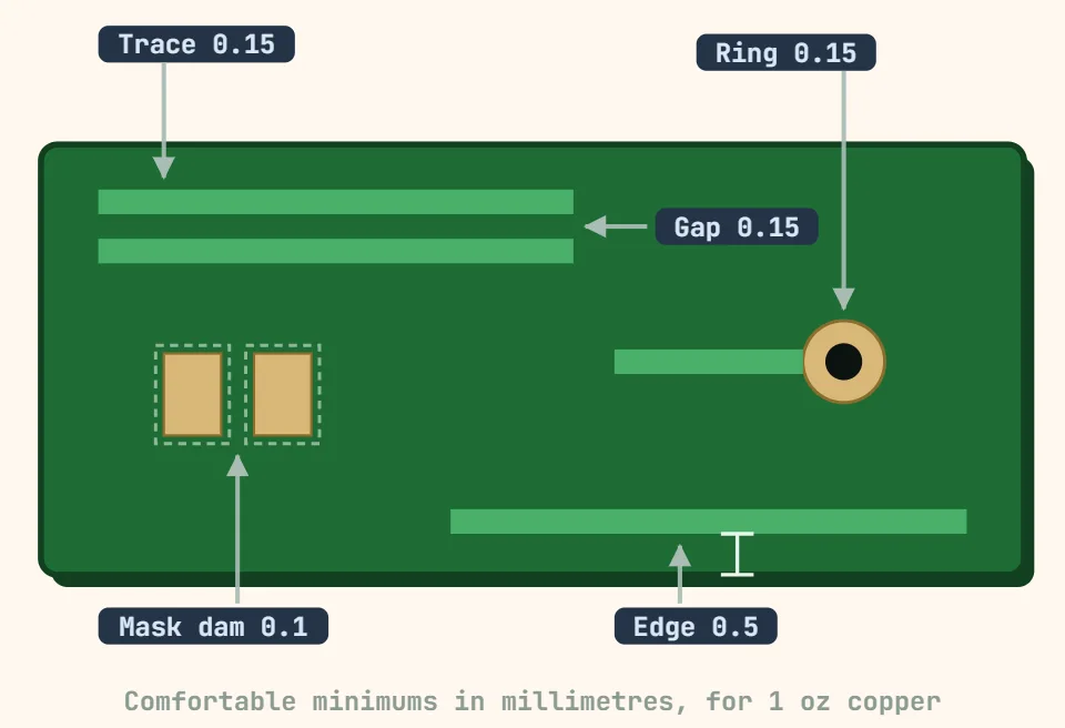
| Trace width / spacing, 1 oz outer | 0.15 mm / 0.15 mm | 0.09 mm / 0.09 mm | Roughly double both for 2 oz copper — thick copper is etched from the sides as well as the top, so the etchant eats a fine trace in half |
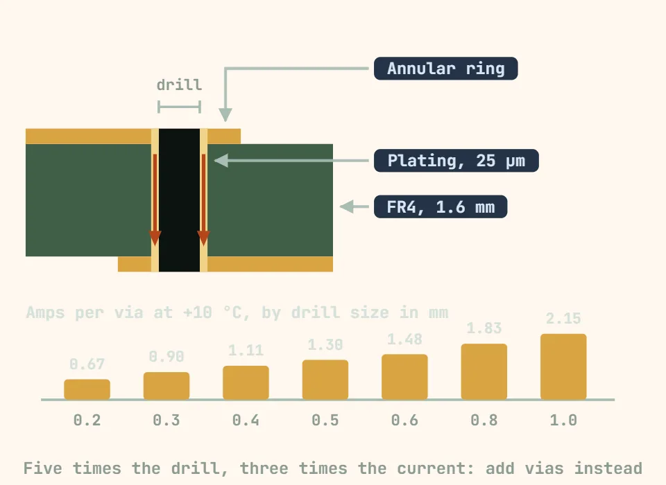
| Annular ring, per side | 0.15 mm | 0.10 mm | Pad diameter = finished hole + twice this. Below 0.1 mm you are paying for breakout scrap |
| Finished hole, via | 0.3 mm | 0.2 mm | Under about 0.15 mm the hole is laser-drilled and priced as a different product |
| Finished hole, component lead | lead Ø + 0.25 mm | lead Ø + 0.15 mm | Too tight and the part will not seat; too loose and the solder never wicks up the barrel |
| Drill sizes | 0.05 mm increments | — | Specify the finished hole and let the fab pick the drill — plating takes roughly 0.05 mm off the diameter |
| Copper to board edge | 0.5 mm | 0.25 mm | The routing bit wanders, and copper exposed at the edge shorts to a metal enclosure |
| Solder mask dam between pads | 0.1 mm | 0.075 mm | Below this the fab drops the dam and the two pads share one opening — the usual cause of fine-pitch bridging |
| Solder mask expansion, per side | 0.05 mm | 0.025 mm | Zero expansion puts mask on the pad as soon as registration drifts |
| Silkscreen line width / text height | 0.15 mm / 1.0 mm | 0.1 mm / 0.8 mm | Thinner disappears in printing, and silk over a pad is removed — taking your designator with it |
| Via in pad | Avoid it | Filled and capped | An open via inside a pad wicks solder off the joint and down the barrel |
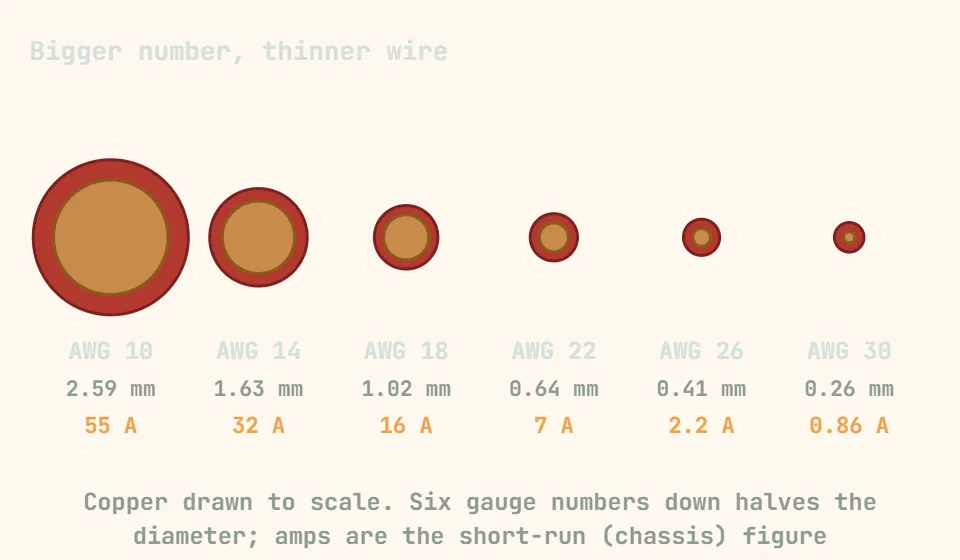
Copper weight is a thickness, not a quality: 1 oz/ft² = 35 µm ≈ 0.5 mΩ per square, 2 oz = 70 µm ≈ 0.25 mΩ per square, 0.5 oz = 17.5 µm ≈ 1 mΩ per square, 3 oz = 105 µm for power boards. At the same width, current scales with the copper to the power 0.725: about 1.65× the 1 oz figures in 2 oz, 2.2× in 3 oz, 0.6× in 0.5 oz — and heavier copper raises most fabs' minimum trace and space, often to 6–8 mil instead of 4–5. "Per square" is shape-independent, so a 0.25 mm trace 25 mm long is 100 squares of 1 oz copper — about 50 mΩ, and half a volt lost at 10 A. Unless you specify otherwise you are getting 1 oz outer layers, and on a cheap 4-layer stack the inner layers are often 0.5 oz, which halves every inner-layer figure above again.