Reference sheet
Abbreviations
SMD, BOM, ESR, PTH: the jargon on datasheets and fab files
Electronics abbreviations & acronyms glossary
Datasheets, fabrication files, and assembly notes for PCBs lean on a dense shorthand of abbreviations. This glossary collects the ones you'll run into most often when reverse-engineering a board or reading its documentation, covering board technologies (SMD, THT), assembly processes (reflow, wave solder, pick-and-place), sourcing and fabrication jargon (BOM, gerber), and compliance or reliability terms (RoHS, ESD, derating).
A few entries describe closely related but distinct ideas, such as footprint versus package or PTH versus NPTH, so it helps to read those side by side if you're not sure which applies. Where a typical number is given, such as a derating percentage, treat it as a common rule of thumb rather than a fixed spec, since exact figures vary by manufacturer, industry, and application; always check the actual part's datasheet.
| Term | Definition |
|---|---|
| BOM | Bill of Materials. The full parts list for a board: reference designator, value, footprint, manufacturer part number, quantity, and often a supplier link. Drives sourcing and assembly, and BOM cost often shapes design choices as much as electrical performance does. |
| Datasheet abs-max (Absolute Maximum Ratings) | The hard limits a manufacturer states a part must never exceed, even briefly, without risking permanent damage or degraded reliability. These are not the conditions the part is meant to run at continuously; check the datasheet's separate 'recommended operating conditions' table for that. |
| Derating | Deliberately operating a component below its absolute maximum rating to improve reliability and lifespan under heat, ripple current, or transients. A common rule of thumb is running parts around 50-80% of their rated value, but the right margin varies by component type, manufacturer, and how conservative the application needs to be (aerospace derates harder than consumer gear). |
| EMI/EMC | Electromagnetic Interference / Electromagnetic Compatibility. EMI is unwanted electrical noise a circuit emits or picks up; EMC is the broader discipline of designing so a device neither emits excessive interference nor is disrupted by interference from others. Shows up in layout choices (trace routing, ground planes, shielding) and in regulatory testing (FCC, CE). |
| ESD | Electrostatic Discharge. A sudden static-electricity transfer that can damage sensitive components, especially CMOS ICs and MOSFETs, sometimes with no visible symptom until the part fails later. Anti-static mats, wrist straps, and ESD-safe packaging are the standard mitigations when handling bare boards or loose parts. |
| ESR | Equivalent Series Resistance. The parasitic resistance inside a capacitor, most relevant for electrolytics, that causes self-heating and voltage ripple under AC current. Lower ESR is generally better for filtering and power-supply work; datasheets list it at a specific frequency since it varies with both frequency and temperature. |
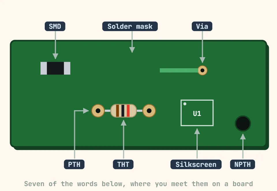
| Footprint | The 2D pattern of pads, silkscreen outline, and (for through-hole parts) drill holes on the PCB where a component is soldered. Has to match the component's physical package exactly in pad size, spacing, and orientation, or the part won't fit or solder reliably. |
| Gerber | The de facto standard file format (RS-274X) that describes each PCB layer, output by CAD tools for fabrication. A full Gerber set plus a drill file is what gets sent to a PCB manufacturer to have boards made. |
| Jellybean part | A common, cheap, widely-stocked component with no special selection requirements, such as a 10 kΩ resistor or a 100 nF ceramic capacitor. Favoring jellybean parts where the design allows it keeps sourcing easy and cost down, especially useful during shortages. |
| NPTH | Non-Plated Through Hole. A drilled hole with no copper plating inside, used for mechanical purposes like mounting screws or alignment pins rather than for making an electrical connection. |
| Package | The physical body and outline of a component (SOIC-8, QFN-32, 0603, and so on), independent of what circuit is inside it. Two parts with completely different functions can share a package, and the same function can be offered in several different packages. |
| PCB | Printed Circuit Board. The fiberglass (or other substrate) board with etched copper traces that mechanically supports and electrically connects the components soldered onto it. |
| Pick-and-place | Both the automated machine that places SMD components onto solder paste on a bare board, and the data file (often called a pick-and-place or centroid file) listing each component's X/Y position, rotation, and board side that drives the machine. |
| PTH | Plated Through Hole. A drilled hole with copper plating on its inner wall, used to connect layers electrically and to anchor and solder a through-hole component's leads. |
| Reflow | The main SMD soldering process: solder paste is printed onto pads, components are placed on top, and the board then passes through a reflow oven with a controlled temperature profile that melts the paste and solders every joint at once. |
| RoHS | Restriction of Hazardous Substances, an EU directive limiting substances like lead, mercury, and cadmium in electronics. RoHS-compliant assembly uses lead-free solder, which has a higher melting point than traditional leaded (tin-lead) solder and behaves a bit differently under a soldering iron. |
| Silkscreen | The printed layer on a PCB, usually white but sometimes another color, showing reference designators, polarity marks, logos, and other text used to identify and orient components during assembly and debugging. It's ink, not a conductor, and carries no electrical function. |
| SMD | Surface-Mount Device. A component designed to be soldered directly onto pads on the board surface with no drilled holes needed. Enables much smaller parts and higher board density than through-hole, and is the dominant assembly style in modern electronics. |
| Solder mask | The protective coating on a PCB, most often green but available in any color, covering the copper everywhere except pads and vias. Prevents solder bridges between adjacent pads during assembly and protects exposed copper traces from oxidation and accidental shorts. |
| THD | Total Harmonic Distortion. A measure of how much unwanted harmonic content an amplifier, converter, or signal chain adds to a signal, usually expressed as a percentage. Lower is better for audio and precision analog work; a well-regarded audio amplifier typically stays well under 1%, though what counts as 'good' depends heavily on the application. |
| THT | Through-Hole Technology. Components with leads inserted through plated holes (PTH) and soldered on the opposite side, by hand or via wave soldering. More mechanically robust than SMD, useful for connectors and parts under physical stress, but bulkier and less dense. |
| Wave solder | An assembly process, mainly for through-hole boards, where the populated board passes over a wave of molten solder that wicks up through the plated holes and coats the leads from below, soldering many joints in a single pass. Still used today, often alongside reflow on boards that mix SMD and THT parts. |
Abs-max ratings and recommended operating conditions are two different tables in the same datasheet; designing right up against the abs-max limit instead of staying inside the recommended range is a common way to quietly shorten a part's lifespan even though it "works" on the bench.