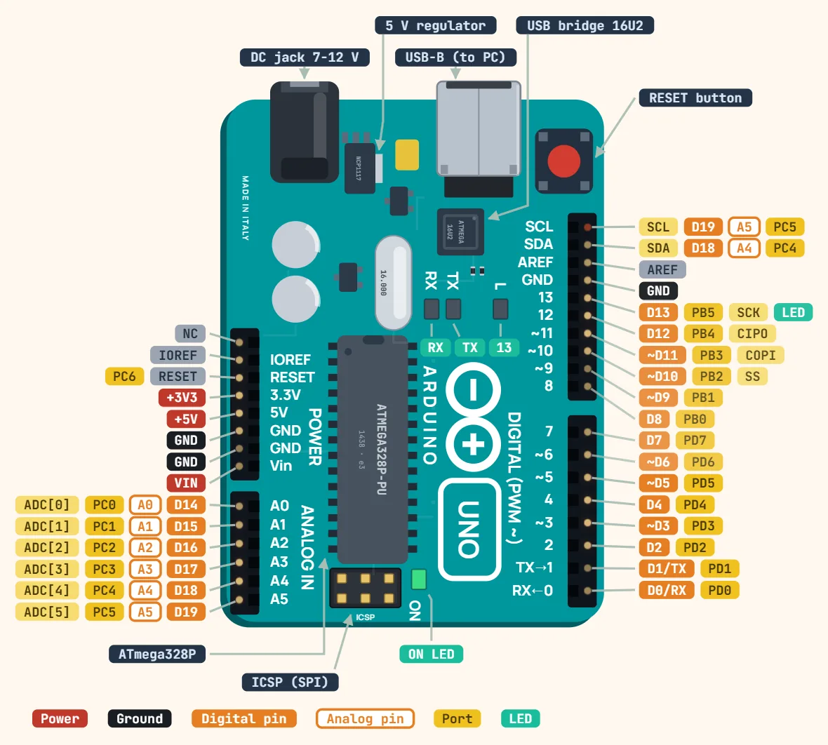
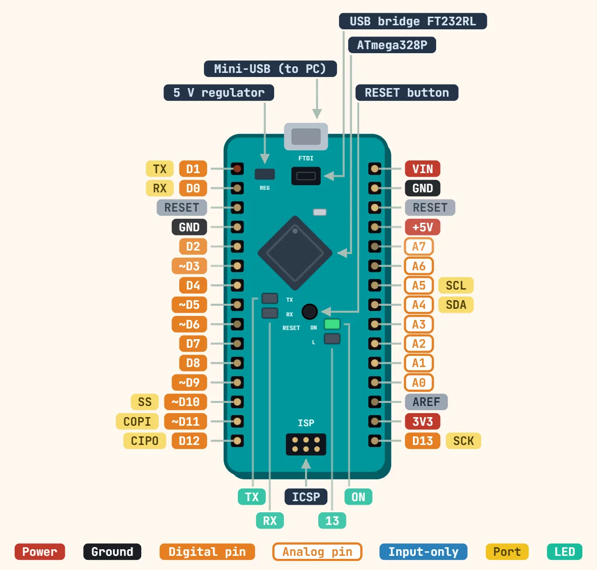
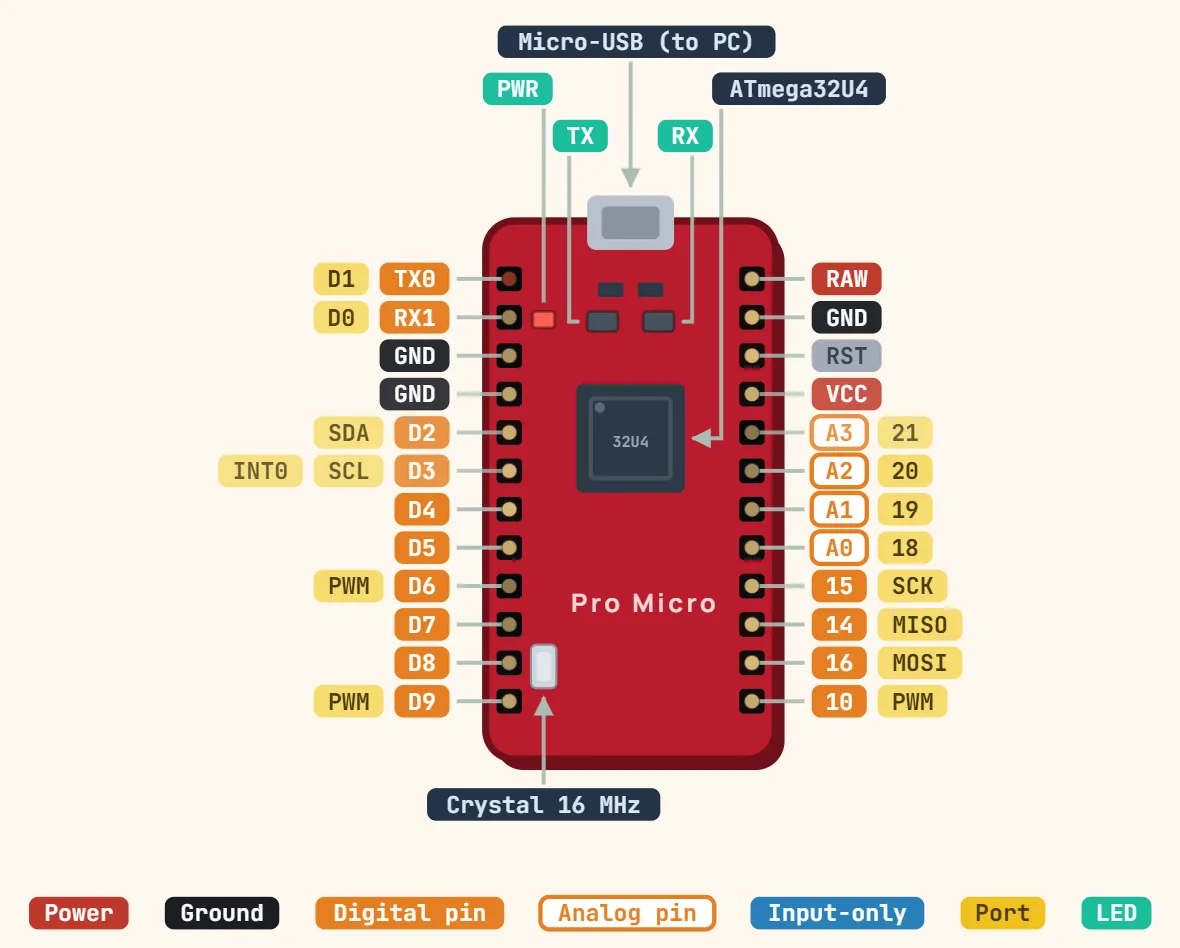
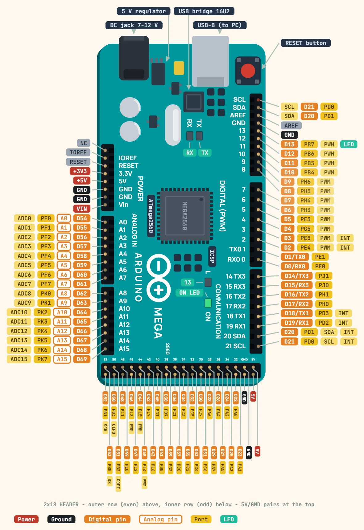
Pinout
Arduino Pro Mini (ATmega328P) pinout
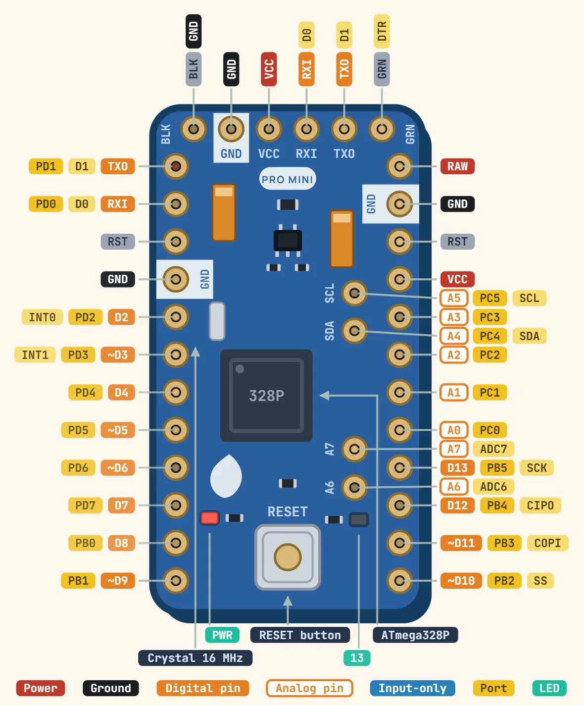
Pins
- TXO — D1 — PD1
- RXI — D0 — PD0
- RST
- GND
- D2 — PD2 — INT0
- ~D3 — PD3 — INT1
- D4 — PD4
- ~D5 — PD5
- ~D6 — PD6
- D7 — PD7
- D8 — PB0
- ~D9 — PB1
- RAW
- GND
- RST
- VCC
- A5 — PC5 — SCL
- A3 — PC3
- A4 — PC4 — SDA
- A2 — PC2
- A1 — PC1
- A0 — PC0
- A7 — ADC7
- D13 — PB5 — SCK
- A6 — ADC6
- D12 — PB4 — CIPO
- ~D11 — PB3 — COPI
- ~D10 — PB2 — SS
- FTDI header: BLK — GND
- FTDI header: GND
- FTDI header: VCC
- FTDI header: RXI — D0
- FTDI header: TXO — D1
- FTDI header: GRN — DTR
Specifications
| Microcontroller | ATmega328P |
|---|---|
| Versions | 3.3 V / 8 MHz or 5 V / 16 MHz |
| Input voltage (RAW) | 3.35–12 V (3.3 V version), 5–12 V (5 V version) |
| Digital I/O pins | 14 (6 PWM) |
| Analog input pins | 8 (A6, A7 analog only) |
| DC current per I/O pin | 20 mA (40 mA absolute max) |
| Flash memory | 32 KB |
| SRAM | 2 KB |
| EEPROM | 1 KB |
| USB | none: program through a 6-pin FTDI adapter |
| Size | 18 × 33 mm |
Notes
- Two 12-pin long rows plus a 6-pin FTDI serial header along the top short edge (BLK = GND, GND, VCC, RXI, TXO, GRN = DTR — the silk prints the FTDI cable’s wire colours at each end). The DTR line is what auto-resets the board for an upload: there is no USB and no USB-to-serial chip on the board at all, so a 3.3V or 5V FTDI cable/breakout is the programmer.
- A4 (SDA) and A5 (SCL) are NOT on the long rows: they are two inboard pads beside the right-hand row, just below VCC and A3. A6 and A7 are two more inboard pads lower down, beside D13 and D12, and are analog-input-only (no digitalWrite). Using I2C on a Pro Mini means soldering a wire or a right-angle pin to those pads.
- RAW takes unregulated input (5–12V on the 5V/16MHz board, 3.35–12V on the 3.3V/8MHz one) into the onboard regulator; VCC is the regulated rail, and feeding a clean 5V (or 3.3V) straight into VCC bypasses that regulator. RST and GND each appear once on both long rows, and the FTDI header adds two more GNDs.
- ~D3, ~D5, ~D6, ~D9, ~D10 and ~D11 are the PWM pins; D13 drives the onboard status LED; D10–D13 are SPI SS / COPI / CIPO / SCK; D2 and D3 are the two external interrupts (INT0/INT1).
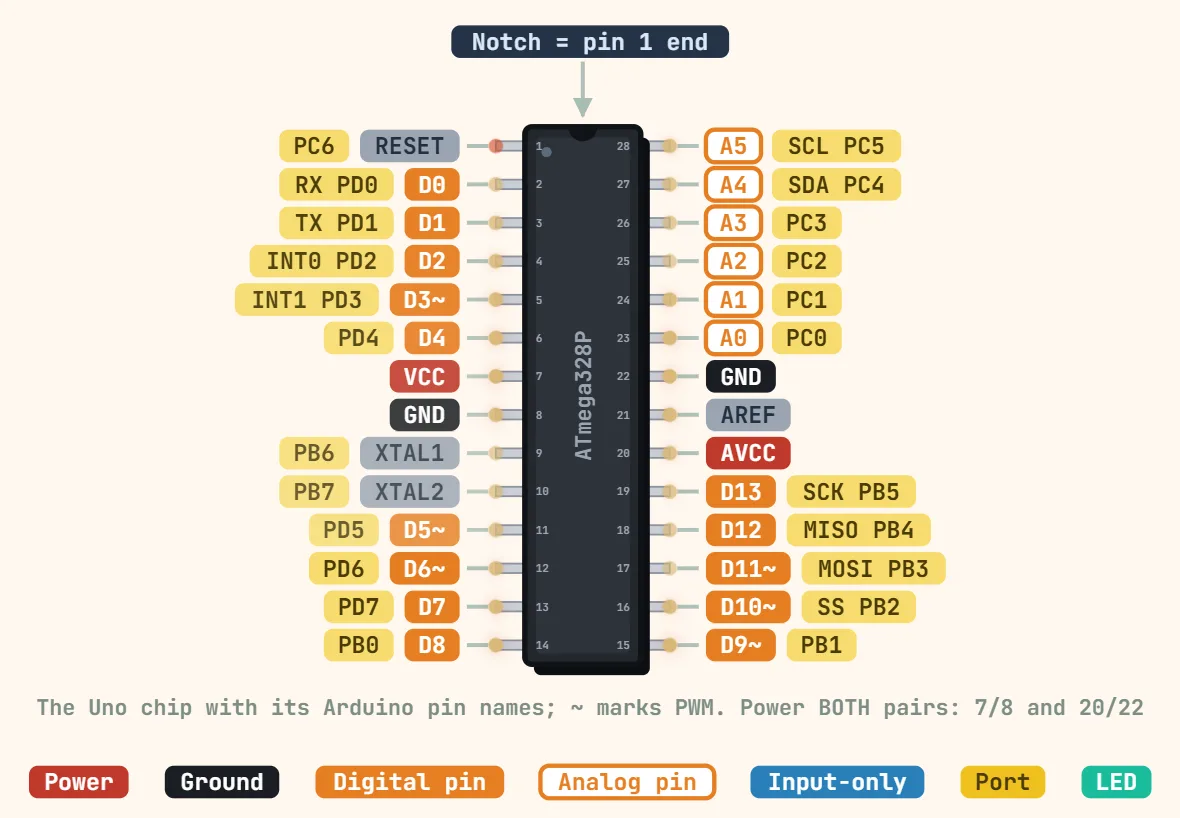
- Same ATmega328P as the Uno/Nano: 40mA absolute maximum per I/O pin, 200mA total across VCC/GND combined.
- The regulator has little headroom to spare (this board runs from a coin cell or a small LiPo more often than the others), so budget any load on VCC conservatively rather than assuming Uno-like regulator margin. The 3.3V version runs at 8 MHz — pick the matching board/processor in the IDE or the serial timing will be wrong.