Pinout
STM32 Blue Pill (F103C8T6) pinout
Pins
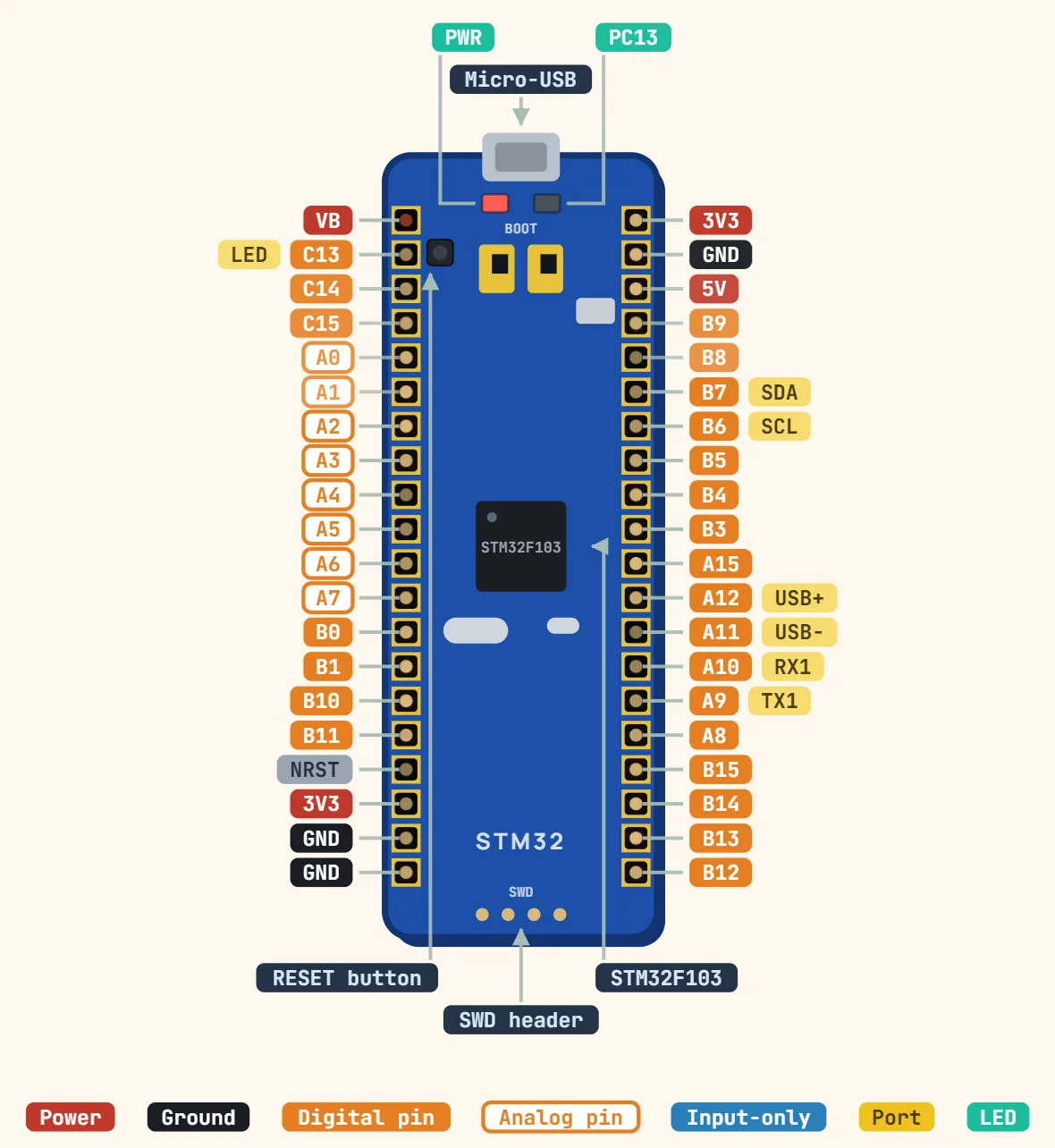
- VB
- C13 — LED
- C14
- C15
- A0
- A1
- A2
- A3
- A4
- A5
- A6
- A7
- B0
- B1
- B10
- B11
- NRST
- 3V3
- GND
- GND
- 3V3
- GND
- 5V
- B9
- B8
- B7 — SDA
- B6 — SCL
- B5
- B4
- B3
- A15
- A12 — USB+
- A11 — USB−
- A10 — RX1
- A9 — TX1
- A8
- B15
- B14
- B13
- B12
Specifications
| Microcontroller | STM32F103C8T6, Arm Cortex-M3 |
|---|---|
| Clock speed | 72 MHz (8 MHz crystal) |
| Flash memory | 64 KB (many chips actually have 128 KB) |
| SRAM | 20 KB |
| Supply | 5 V pin or USB, onboard 3.3 V regulator |
| Logic level | 3.3 V (FT pins are 5 V tolerant) |
| GPIO current | 25 mA absolute max per pin, 150 mA total |
| PC13–PC15 | 3 mA sink max, 2 MHz max |
| ADC | 2 × 12-bit, 10 channels |
| Peripherals | 3 × USART, 2 × SPI, 2 × I2C, CAN, USB full-speed |
| USB | Micro-USB, native (no USB-serial chip) |
| Programming | SWD header or serial bootloader on USART1 |
Boot & strapping
- BOOT0 = 0 (its normal resting position): boots from the main flash — where it should sit for everyday use.
- BOOT0 = 1 with BOOT1 = 0: boots the chip’s built-in serial bootloader instead, which flashes new firmware over USART1 (PA9/PA10) through a USB-to-serial adapter — no ST-Link needed.
- BOOT0 = 1 with BOOT1 = 1 boots from embedded SRAM instead of flash, rarely what you want. Most boards expose BOOT1 as a second small jumper right next to BOOT0 — check both before assuming a board is stuck.
- After flashing through the serial bootloader, move BOOT0 back to 0 and reset or power-cycle the board — the new firmware will not run while BOOT0 still points at the bootloader.
- An SWD debugger (ST-Link) ignores BOOT0/BOOT1 entirely and can flash or debug regardless of jumper position — the jumpers only matter for the USB-to-serial flashing path.
Notes
- Logic is 3.3V. Most GPIOs are NOT 5V tolerant — only PA8–PA15, PB3/PB4, PB6–PB15 and PC6–PC15 are FT (5V-tolerant); every ADC-capable pin (PA0–PA7, PB0, PB1, PB5, PC0–PC5) is 3.3V-only and can be damaged by 5V.
- PC13, the onboard LED pin, is active-LOW and — like the whole PC13–PC15 group — can only sink about 3mA at up to 2MHz through the backup-domain power switch; never use it as a current source for anything beyond that one onboard LED.
- Every other GPIO is rated 20mA per pin (a relaxed spec pushes this to 25mA, at reduced output voltage), but the whole package is capped around 150mA combined — much less headroom to spread across many pins at once than an AVR board’s 200mA, despite the similar-looking per-pin figure.
- Some boards genuinely carry a different, non-ST chip (CS32F103 and similar clones) that can misbehave on USB or DMA-heavy peripherals — check the reported Device ID in your programmer if something is unreliable. That is separate from a genuine ST die reporting 128KB instead of the datasheet’s 64KB, which is usually just relabeled surplus silicon and not a fake.
- There is no standard numbered header position on this board either: every reference names pins PA0…PC15 by their MCU name, never by a position number.