Free online calculator
NE555 timer calculator
Astable
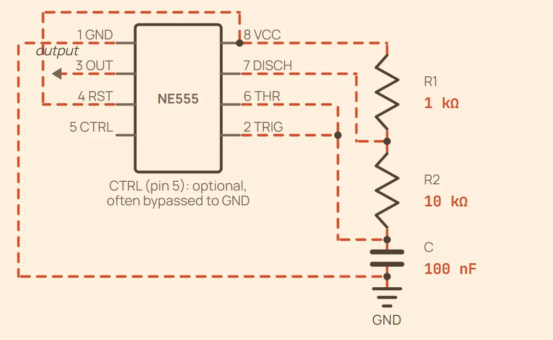
Fully wired timing network — pins are grouped by function, not physical DIP order (see the 555 timer entry in Pinouts for the real pin layout). RST is tied to VCC to keep the chip enabled; OUT is the square-wave output (goes to whatever load you're driving); CTRL is left as noted since it's optional for basic operation.
Example Frequency: 685.7 Hz — duty cycle: 52.38 %
Duty cycle — reported below as a percentage. It can never reach 50 %: the capacitor charges through R1 + R2 but discharges through R2 alone, so the high phase is always the longer one.
What you enter
- R1 (Ω)
- R2 (Ω)
- C
Monostable
Fully wired timing network — pins are grouped by function, not physical DIP order (see the 555 timer entry in Pinouts for the real pin layout). Pin 2 (TRIG) is not part of the R/C network — it needs a separate external trigger pulse. RST is tied to VCC to keep the chip enabled; OUT is the pulse output; CTRL is left as noted since it's optional for basic operation.
Example Pulse width: 110 ms
One-shot pulse width: — the pulse starts when pin 2 (TRIG) is pulled below ⅓ Vcc.
What you enter
- R (Ω)
- C
Bistable
Pins grouped by function, not physical DIP order (see the 555 timer entry in Pinouts for the real pin layout). Pulling SET below ⅓ Vcc latches OUT high; pulling RESET above ⅔ Vcc latches OUT low. DISCH (pin 7) is left unconnected — there's no timing capacitor to discharge in this mode. RST (pin 4) is tied to VCC to keep the chip enabled.
Example No timing formula in this mode — OUT just follows whichever input (SET/RESET) was driven most recently. 10 kΩ is a typical pull resistor value; lower it if noise is falsely triggering an input.
No timing capacitor — SET (pin 2) and RESET (pin 6) are level-controlled inputs, each held to its resting state by a pull resistor until driven the other way.
What you enter
- Pull-up R — SET (Ω)
- Pull-down R — RESET (Ω)