مخطط الأطراف
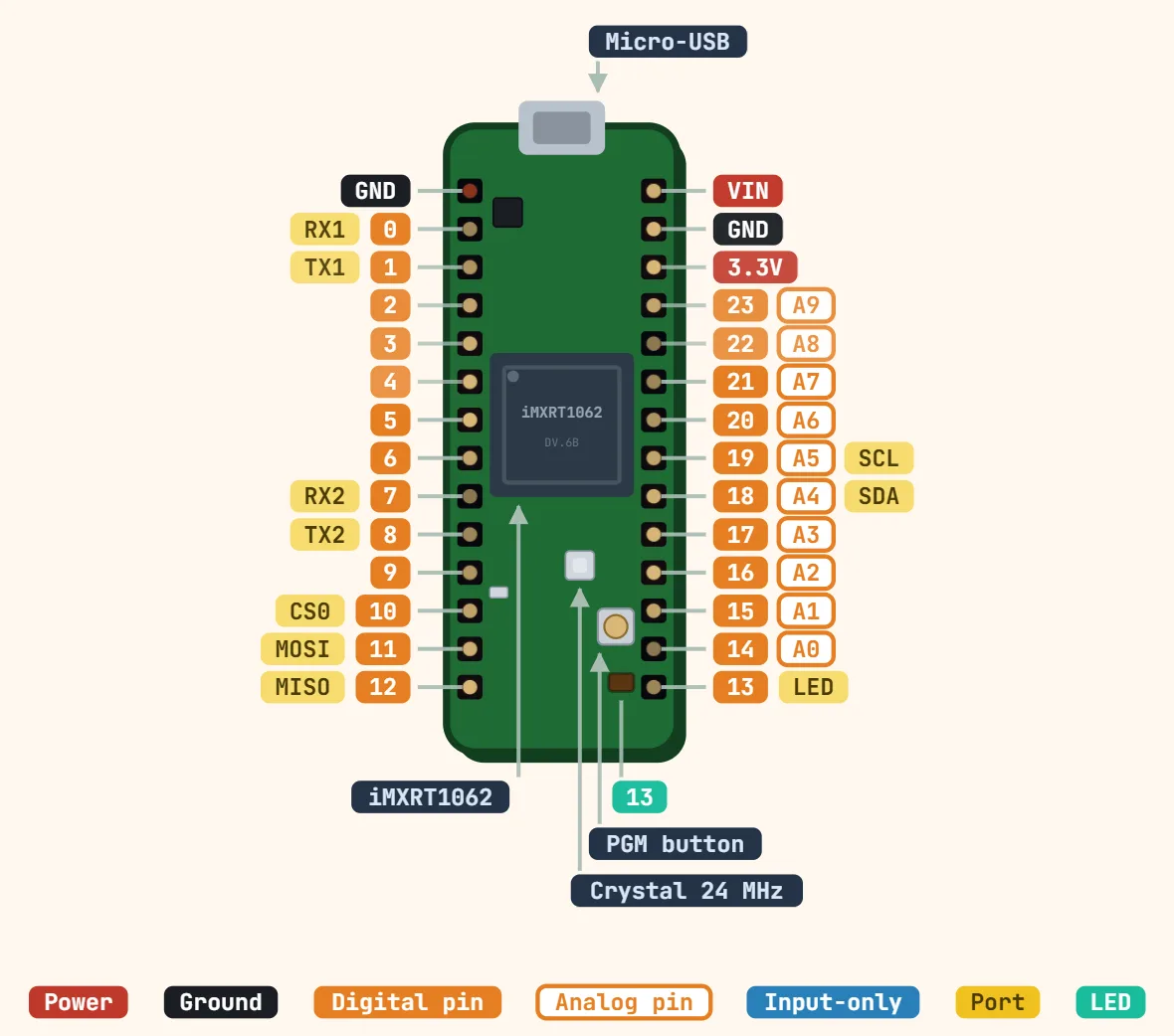
مخطط أطراف Teensy 4.0
الأطراف
- GND
- 0 — RX1
- 1 — TX1
- 2
- 3
- 4
- 5
- 6
- 7 — RX2
- 8 — TX2
- 9
- 10 — CS0
- 11 — MOSI
- 12 — MISO
- VIN
- GND
- 3.3V
- 23 — A9
- 22 — A8
- 21 — A7
- 20 — A6
- 19 — A5 — SCL
- 18 — A4 — SDA
- 17 — A3
- 16 — A2
- 15 — A1
- 14 — A0
- 13 — LED
المواصفات
| Processor | NXP i.MX RT1062, Arm Cortex-M7 |
|---|---|
| سرعة الساعة | 600 MHz |
| RAM | 1024 KB (512 KB tightly coupled) |
| ذاكرة Flash | 2048 KB (64 KB reserved for recovery and EEPROM emulation) |
| Supply (VIN) | 3.6–5.5 V |
| المستوى المنطقي | 3.3 V (لا يتحمل 5 V) |
| Output current | 4 mA recommended per pin |
| Digital pins | 40 total (24 on the main header), 31 PWM |
| Analog inputs | 14 (10 on the main header) |
| Serial ports | 7 × UART, 3 × SPI, 3 × I2C, 3 × CAN (1 CAN FD) |
| USB | Micro-USB, 480 Mbit/s device |
| الأبعاد | 35.6 × 17.8 mm |
الملاحظات
- Every pin — digital and analog alike — is 3.3V logic and NOT 5V tolerant. PJRC’s own documentation says it plainly: never drive any pin above 3.3V. A 5V sensor or shield built for an Uno or Mega needs a level shifter or a divider first, not a direct connection.
- PJRC’s recommended maximum output current is only 4mA per pin — well below the ~20–40mA headroom a typical AVR board like the Uno tolerates. Driving an LED straight off a pin the way a beginner Arduino tutorial shows will overdrive it here; size the series resistor for 4mA, or use a transistor/driver IC for anything more. 31 of the 40 total digital pins support PWM output — check a specific pin against PJRC’s own reference card before assuming it does.
- No WiFi or Bluetooth on this board (that’s the Teensy 4.1, or an add-on module) — the 4.0 is a bare Cortex-M7 running at 600MHz, the fastest clock of any board in this tab, but with zero onboard radio.
- The on-chip I2C pull-ups are, in PJRC’s own words, “very weak” on this chip — Wire, Wire1 and Wire2 all want external 1k–4.7k resistors to 3.3V for anything beyond the slowest, shortest bus, unlike boards where the internal pull-ups are usable as-is.
- VIN and VUSB (a separate solder pad, raw 5V straight off the USB connector, not on the main header) share a single net on the Teensy 4.0 — powering the board from an external 5V supply on VIN while it is still plugged into USB can push current back out through the USB port and into whatever is on the other end of the cable. The 4.1 adds a cuttable trace to separate them; the 4.0 doesn’t.
- Pin 13 is the default SPI SCK and also drives the onboard orange LED, so it flickers whenever the default SPI bus is active — PJRC explicitly warns against pinMode INPUT_PULLUP here, since an external signal would then have to fight the LED’s own drive.
- This map shows only the front 28-pin (2×14) header (pins 0–23), which is everything PJRC calls "easily accessible." Pins 24–39 — including analog inputs A10–A13, Serial6 (24/25, doubling as Wire2 SCL/SDA), and Serial7 (28/29) — exist only as castellated pads on the back of the board, not on this header; A12/A13 are additionally ADC2-only, unlike every other analog pin here which can be read from either onboard ADC.
- Most of the extra SPI/I2C/UART ports and the CAN pins are multiplexed onto the same physical header pins shown here, so more than one peripheral can be configured onto a given pin in code even though only one can actually use it at a time — check which function a sketch is really claiming before assuming a pin is free for something else.
- ON/OFF and VBAT are dedicated pads, not part of the main header: ON/OFF takes a normally-open pushbutton to GND for a soft power switch (hold ~4s to cut the 3.3V rail, a short press turns it back on and reboots), and VBAT is a coin-cell backup input that keeps the RTC running and remembers ON/OFF power state through a loss of VIN/VUSB — with no cell fitted, the board just powers back on by default when power returns.