इंटरैक्टिव सिमुलेशन
क्लास-AB क्रॉसओवर सिमुलेशन
हर ज़ीरो क्रॉसिंग पर सुनाई देने वाला नॉच, और उसे बंद करने वाला बायस करंट।
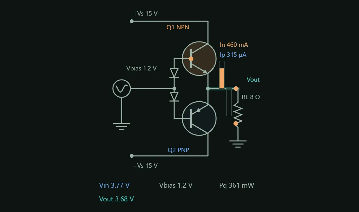
Each transistor is an emitter follower that only conducts on its own half of the wave: the NPN pushes, the PNP pulls. Pull the bias to 0 V and neither one is on until the input has climbed past its Vbe, so the output sits at zero through a dead band roughly 1.3 V wide — that flat step at every zero crossing is the crossover notch, and the red error trace shows it flipping sign twice per cycle. That is what you hear: a distortion that is worst at low volume, because the notch is a fixed number of volts wide no matter how small the signal is. Bias the two bases about 1.2 V apart and both devices idle at a few tens of milliamps; the handover becomes continuous, the notch closes and THD collapses. Push further and nothing improves — you only burn Pq = 2·Vs·Iq in the heatsink, which is how output stages cook themselves.
आप क्या बदल सकते हैं
- Supply rail Vs