पिनआउट
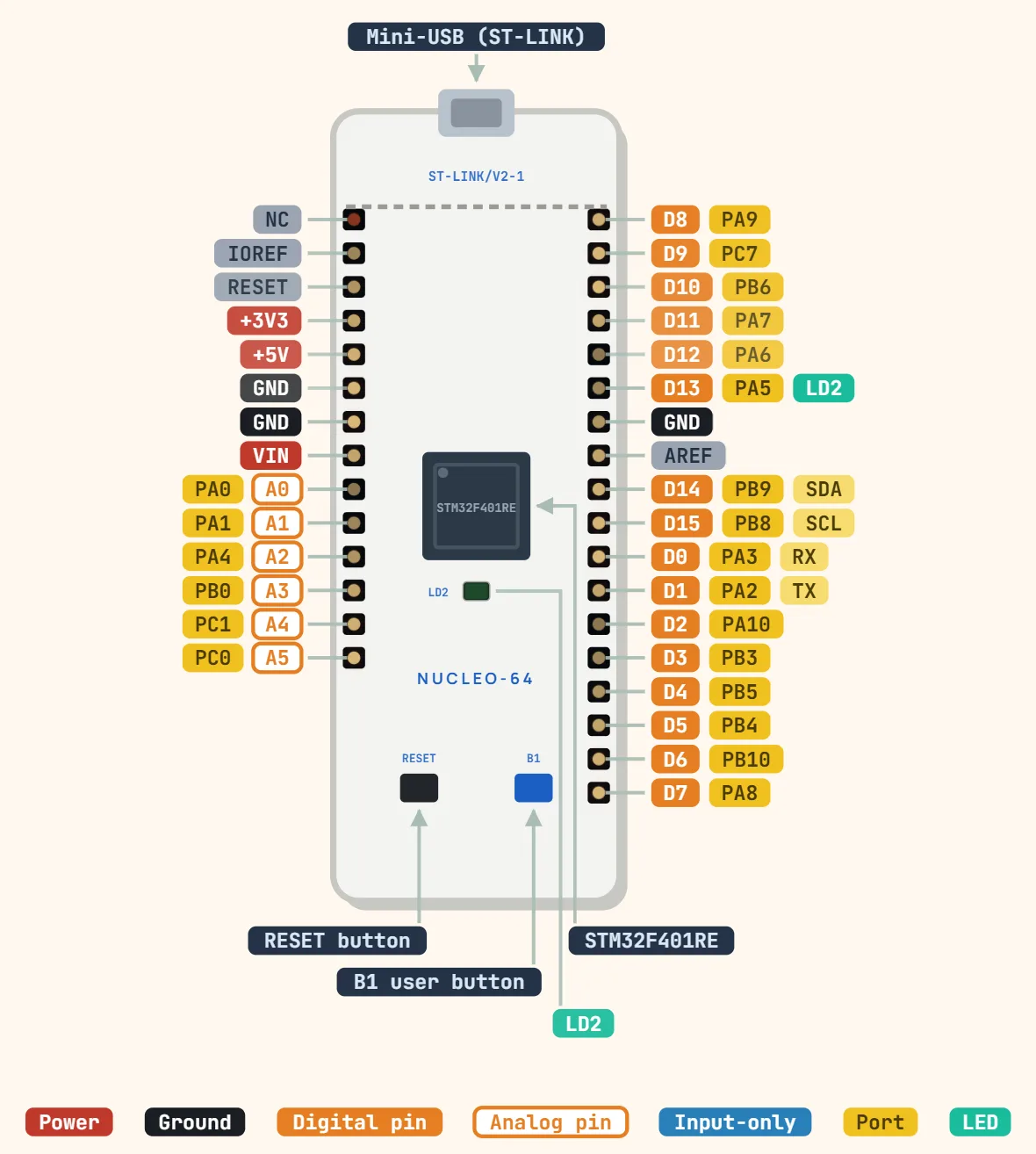
STM32 Nucleo-64 (जैसे NUCLEO-F401RE) पिनआउट
पिन
- NC
- IOREF
- RESET
- +3V3
- +5V
- GND
- GND
- VIN
- A0 — PA0
- A1 — PA1
- A2 — PA4
- A3 — PB0
- A4 — PC1
- A5 — PC0
- D8 — PA9
- D9 — PC7
- D10 — PB6
- D11 — PA7
- D12 — PA6
- D13 — PA5 — LD2
- GND
- AREF
- D14 — PB9 — SDA
- D15 — PB8 — SCL
- D0 — PA3 — RX
- D1 — PA2 — TX
- D2 — PA10
- D3 — PB3
- D4 — PB5
- D5 — PB4
- D6 — PB10
- D7 — PA8
विनिर्देश
| माइक्रोकंट्रोलर | STM32F401RET6, Arm Cortex-M4F (F401RE) |
|---|---|
| क्लॉक स्पीड | 84 MHz |
| फ़्लैश मेमोरी | 512 KB |
| SRAM | 96 KB |
| लॉजिक लेवल | 3.3 V (FT pins are 5 V tolerant) |
| पावर इनपुट | USB 5 V, or VIN 7–12 V |
| Headers | Arduino Uno V3 + 2 × 38-pin ST Morpho |
| Programmer | On-board ST-LINK/V2-1 (SWD, virtual COM, mass storage) |
| ADC | 12-bit, 16 channels |
| USB | Mini-B (ST-LINK) |
| User I/O | LD2 green LED (PA5), B1 user button (PC13) |
नोट्स
- The whole ST-LINK/V2-1 section of the board is a real standalone SWD programmer, not just a convenience: snap it off along the scored perforation between the two halves (or leave them joined and just run jumper wires to CN4) and it will flash and debug any external STM32 target, not only this board's own MCU.
- The ST-LINK's USB virtual COM port is wired to the target's USART2 by default (PA2 TX / PA3 RX — the same two pins as Arduino header D1/D0), so Serial output read back over the USB cable and any other use of D0/D1 for a different UART are contending for the same physical pins.
- LD2 (the green USER LED) and Arduino pin D13 sit on the same net, PA5, which is also the default SPI1 SCK pin on most Nucleo-64 boards — an SPI shield using hardware SPI1 will visibly flicker the LED as a side effect, and code that toggles D13 fast will inject noise onto that SPI clock line.
- Logic is 3.3V, and exactly which STM32 GPIO lands on each Arduino-header pin (D0–D15, A0–A5) — plus which pins are 5V-tolerant, per the datasheet's own 'FT' markings — is fixed by ST per Nucleo-64 variant, not a universal Nucleo-64 constant: the F401RE's pinout table is not the F446RE's or the L476RG's.
- A4/A5 default to PC1/PC0 at the factory (plain ADC1 channels); a solder-bridge rework documented in ST's own manual can swap them to PB9/PB8 instead, exposing them as a second I2C1 (SDA/SCL) pair sharing the same physical pins as the digital header's own D14/D15 — don't assume A4/A5 are free analog pins on a board that's had this rework done.
- Morpho CN7 / CN10 — two 38-pin (2×19) headers giving near-total access to the STM32 package's pins, well beyond what the Arduino header alone exposes; not covered by this pin map, which only draws the Arduino-compatible header.
- NRST is tied to the black RESET button and to the ST-LINK's own reset control; B1, the blue USER button, is wired to PC13 on the F401RE, a GPIO the ST-LINK doesn't touch.
- JP6 (IDD) — a jumper in series with the MCU's own 3.3V rail on most Nucleo-64 boards; remove it and bridge an ammeter across the two pins to measure the target's real current draw.