पिनआउट
MCP23017 I2C GPIO एक्सपैंडर पिनआउट
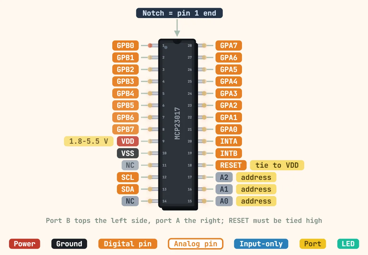
पिन
- 1–8: GPB0–GPB7 — Port B, 8 individually configurable I/O pins (each set as input or output per-bit via IODIRB), with an internal ~100kΩ weak pull-up selectable per pin (GPPUB) when configured as an input
- 21–28: GPA0–GPA7 — Port A, an identical second 8-bit bank with the same per-pin direction, pull-up and interrupt-on-change controls as Port B
- 9: VDD — supply, 1.8–5.5V
- 10: VSS — ground
- 12: SCL — I2C clock, open-drain like any I2C line, needs a pull-up
- 13: SDA — I2C data, open-drain, same pull-up requirement as SCL
- 15–17: A0–A2 — hardware address select pins; combined with a fixed 0100 prefix they set the 7-bit I2C address, from 0x20 with all three tied low up to 0x27 with all three tied high — tie each one firmly to VDD or VSS, they float rather than self-bias
- 18: RESET# — active-low hardware reset; must be tied to VDD for the chip to respond on the bus at all, and pulsed low to reset it
- 19: INTA — interrupt output, fires on an enabled change on any Port A pin
- 20: INTB — interrupt output for Port B; INTA and INTB can be tied together and wire-ORed onto a single shared line (IOCON.MIRROR) instead of running two separate interrupt lines back to the MCU
- 11, 14: NC — no internal connection on this I2C part; on the pin-compatible SPI variant (MCP23S17) pin 11 becomes CS
विनिर्देश
| सप्लाई वोल्टेज | 1.8–5.5 V |
|---|---|
| इंटरफ़ेस | I2C: 100 kHz, 400 kHz, 1.7 MHz |
| I2C address | 0x20–0x27 (set by A0–A2) |
| I/O | 16 pins in two 8-bit ports (A and B) |
| पुल-अप रेज़िस्टर | ≈ 100 kΩ internal, selectable per pin |
| Output current | 25 mA per pin; 125 mA total into VDD, 150 mA total out of VSS |
| Interrupts | 2 outputs (INTA, INTB), can be mirrored |
| Standby current | 1 µA max |
| Operating temperature | −40–125 °C (E grade) |
| पैकेज | DIP-28, SOIC-28, SSOP-28, QFN-28 |
नोट्स
- The base I2C address block is 0x20–0x27, the exact same range used by the PCF8574 port expander — an MCP23017 and a PCF8574 wired to the same A0–A2 combination will collide on the same bus.
- RESET (pin 18) has no internal pull-up: on a bare DIP/SOIC chip, leaving it floating holds the device permanently in reset so it never answers on the bus, which looks exactly like a wiring or address mistake. Most ready-made breakout boards add that pull-up for you; a chip on a custom PCB needs it added explicitly.
- Each GPIO can source or sink roughly 25mA, but that's a per-pin figure, not a per-pin-times-16 budget — the datasheet's absolute maximum ratings cap the whole package at about 125mA total into VDD and 150mA total out of VSS, so driving many pins near their individual limit at once can exceed the chip's overall rating.
- There's a pin-compatible SPI sibling, the MCP23S17, in the same 28-pin package — SDA/SCL on this I2C part become SDI/SDO/SCK/CS on that one, so grabbing the wrong datasheet or library for an unlabeled breakout board is an easy mix-up.