पिनआउट
74HC14 हेक्स श्मिट-ट्रिगर इन्वर्टर (DIP-14) पिनआउट
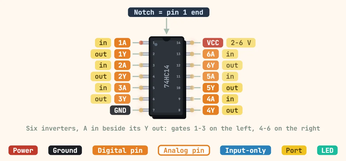
पिन
- 1: 1A — gate 1 input; every input on this chip is a Schmitt trigger, so it tolerates a slow ramp or a noisy line that would make a plain inverter chatter
- 2: 1Y — gate 1 output, the inverted version of 1A (HIGH in → LOW out, and vice versa, on all six gates)
- 3: 2A — gate 2 input, wired identically to 1A
- 4: 2Y — gate 2 output
- 5: 3A — gate 3 input
- 6: 3Y — gate 3 output
- 7: GND — the only ground pin; put a 0.1µF ceramic decoupling cap right at the package, between here and pin 14
- 8: 4Y — gate 4 output
- 9: 4A — gate 4 input
- 10: 5Y — gate 5 output
- 11: 5A — gate 5 input
- 12: 6Y — gate 6 output
- 13: 6A — gate 6 input
- 14: VCC — supply, 2–6V across the HC family (5V is the usual choice); it is the only other power pin, diagonally opposite GND like most 7400-series logic
विनिर्देश
| Logic family | 74HC (high-speed CMOS) |
|---|---|
| Gates | 6 Schmitt-trigger inverters |
| सप्लाई वोल्टेज | 2–6 V |
| Hysteresis | ≈ 0.9 V typ at 4.5 V (thresholds vary by manufacturer) |
| Output current | ±4 mA specified at 4.5 V; ±25 mA absolute max per pin |
| Propagation delay | ≈ 11–12 ns typ at 5 V |
| Quiescent current | 2 µA max at 25 °C (inputs at a rail) |
| Input rise/fall time | No limit (Schmitt inputs) |
| पैकेज | DIP-14, SOIC-14, TSSOP-14 |
नोट्स
- Pin-for-pin identical to a plain 74HC04 hex inverter — same 14 pins, same six inverters, same GND/VCC on 7/14. The only difference is the Schmitt-trigger hysteresis on every input, so a 74HC14 drops straight into a 74HC04 footprint to add noise rejection, and a 74HC04 datasheet is a fair stand-in for anything here that is not about the switching thresholds (drive current, propagation delay, supply range).
- That hysteresis is the entire reason to reach for this part over a plain gate: a standard inverter's datasheet gives a maximum input rise/fall time, and feeding it a slow or noisy edge can make the output oscillate while the input dwells near the switching point. A Schmitt-trigger input has no such limit, which is why the 74HC14 is the go-to for debouncing a mechanical switch, cleaning up an RC-charged input, or squaring up a slow sensor edge.
- The two thresholds are not symmetric around VCC/2 — that gap is the hysteresis. On a typical 5V datasheet the positive-going threshold VT+ is roughly 2.9V and the negative-going VT− roughly 1.7V, so about 1V of hysteresis band; the exact numbers vary a fair bit between manufacturers (TI, Nexperia, ON Semi all publish slightly different typicals), so check your specific datasheet before relying on an exact figure.
- Every unused gate input must be tied HIGH or LOW — never left floating. A floating CMOS input sits near the switching threshold, both halves of the input transistor pair partially conduct at once, and that one gate's supply current jumps from microamps to several mA; on a hex chip with several gates unused, that adds up and can also make the whole package run noticeably warm.
- Output drive is modest, typically only a few mA per pin at 5V (per most HC-family datasheets) — enough to feed another logic input or a small LED through a series resistor, but not a relay coil, a motor, or anything else that wants real current; buffer through a transistor or driver IC instead.
- A single gate with a resistor from output back to input and a capacitor from that input to ground is a classic one-gate RC relaxation oscillator — because the input is a Schmitt trigger it oscillates cleanly at a predictable rate, which a plain 74HC04 gate cannot do reliably on its own.