Brochage
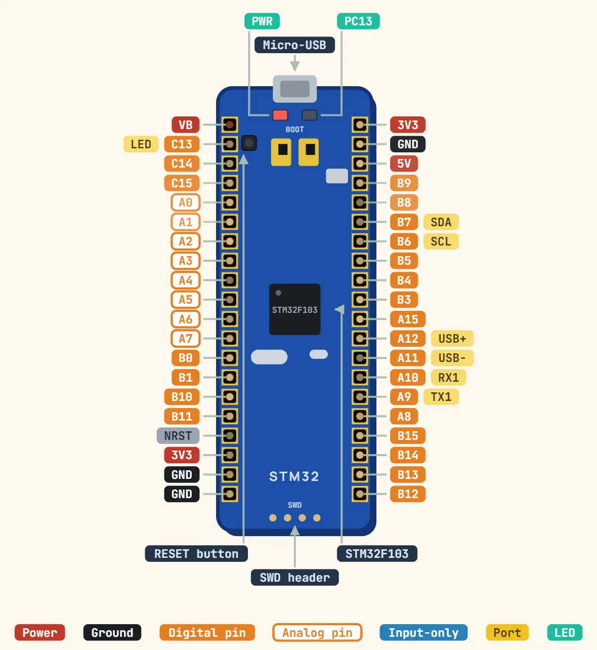
Brochage STM32 Black Pill (WeAct V3.0, F411CEU6)
Broches
- 3V3 — output of the on-board 3.3V LDO (a ~500mA SOT-23-5 part, not the SOT-223 AMS1117 of the Blue Pill); expect only a couple of hundred mA of headroom for peripherals once the MCU has taken its share. It also works as a 3.3V INPUT to power the board directly — but then never plug USB in at the same time, you would back-feed the regulator
- 5V — tied to the USB VBUS rail and feeds the 3.3V LDO (safe input roughly 4.5–6V). Nothing on the MCU itself runs at 5V
- GND — several ground pins on both headers; use the one nearest your signal
- VB — VBAT, the backup-domain supply for the RTC (1.65–3.6V). Leave it open or tie it to 3V3 if you are not fitting a coin cell
- NRST — active-low reset, with an on-board pull-up and the reset button. Pull LOW to reset, never drive it high
- PC13 — on-board user LED, ACTIVE LOW (LED sits between 3V3 and the pin, so writing 0 lights it). Like PC14/PC15 it is a backup-domain pin: max ~3mA and ~2MHz, so never drive a load from it
- PC14 — OSC32_IN. Only free as a GPIO if the 32.768kHz LSE crystal is not fitted (most V3.0 boards ship with it fitted); same ~3mA / 2MHz limit as PC13
- PC15 — OSC32_OUT, same story and same ~3mA / 2MHz limit as PC14
- PA0 — on-board KEY user button, plus WKUP and ADC1_IN0. The button shorts PA0 to one rail: confirm with a continuity check which one before you choose a pull-up or pull-down
- PA2 — USART2_TX (AF7)
- PA3 — USART2_RX (AF7)
- PA4 — SPI1_NSS, and the chip-select for the unpopulated W25Q SPI-flash footprint on the back of the board
- PA5 — SPI1_SCK (AF5)
- PA6 — SPI1_MISO (AF5)
- PA7 — SPI1_MOSI (AF5)
- PA9 — USART1_TX (AF7), the usual serial console pin for a USB-UART adapter — 3.3V levels only
- PA10 — USART1_RX (AF7); this one is an input from a 3.3V or level-shifted source
- PA11 — USB_DM (D−), hard-wired to the USB-C socket; unusable as a GPIO whenever USB is in use
- PA12 — USB_DP (D+), same restriction as PA11
- PA13 — SWDIO on the 4-pin SWD header (3V3, SWDIO, SWCLK, GND). Do not reassign it as a GPIO unless you have another way to reflash the chip
- PA14 — SWCLK on the SWD header, same warning as PA13
- PB2 — general-purpose GPIO but also BOOT1: it must be LOW at reset for the BOOT0 button to enter the DFU bootloader (BOOT0 high with BOOT1 high boots from SRAM instead), so avoid an external pull-up here
- PB6 — I2C1_SCL (AF4). No pull-ups on the board: add 4.7kΩ to 3V3 on both lines
- PB7 — I2C1_SDA (AF4), same pull-up requirement as PB6
- BOOT0 — button (and pad) tied to the MCU's BOOT0 pin. Hold BOOT0, tap NRST, release BOOT0 to drop into the built-in USB DFU bootloader; it is pulled low otherwise so the board boots from flash
- The 25MHz crystal (not the Blue Pill’s 8MHz) sits on PH0/PH1, which reach no header: set HSE_VALUE to 25000000 and size the PLL for it, or every clock and UART baud rate is wrong.
Caractéristiques
| Microcontrôleur | STM32F411CEU6, Arm Cortex-M4F |
|---|---|
| Fréquence d'horloge | 100 MHz (25 MHz crystal) |
| Mémoire flash | 512 KB |
| SRAM | 128 KB |
| Alimentation | 5 V via USB-C or 5V pin, onboard 3.3 V LDO |
| Niveau logique | 3.3 V (FT pins are 5 V tolerant) |
| Courant GPIO | 25 mA absolute max per pin |
| ADC | 12-bit, 10 external channels |
| Périphériques | 3 × USART, 5 × SPI/I2S, 3 × I2C, USB OTG full-speed |
| USB | USB-C, native (DFU bootloader via BOOT0) |
| Programming | SWD header or USB DFU |