Simulación interactiva
Distorsión de cruce clase AB
La muesca que se oye en cada paso por cero, y la corriente de polarización que la elimina.
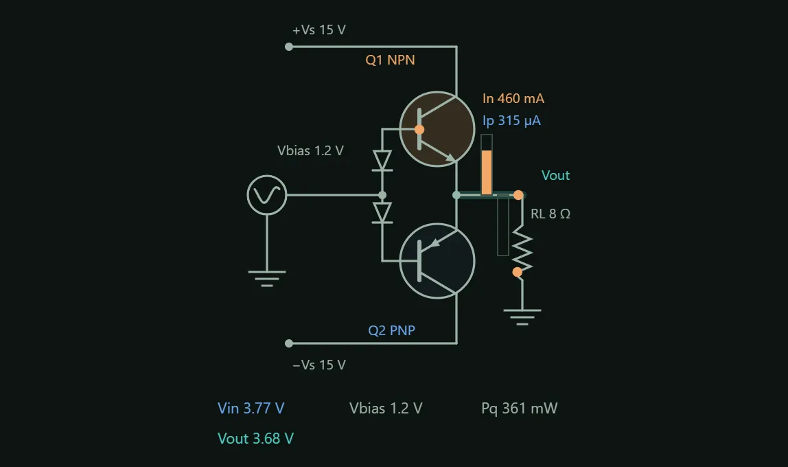
Each transistor is an emitter follower that only conducts on its own half of the wave: the NPN pushes, the PNP pulls. Pull the bias to 0 V and neither one is on until the input has climbed past its Vbe, so the output sits at zero through a dead band roughly 1.3 V wide — that flat step at every zero crossing is the crossover notch, and the red error trace shows it flipping sign twice per cycle. That is what you hear: a distortion that is worst at low volume, because the notch is a fixed number of volts wide no matter how small the signal is. Bias the two bases about 1.2 V apart and both devices idle at a few tens of milliamps; the handover becomes continuous, the notch closes and THD collapses. Push further and nothing improves — you only burn Pq = 2·Vs·Iq in the heatsink, which is how output stages cook themselves.
Lo que puedes cambiar
- Supply rail Vs