पिनआउट
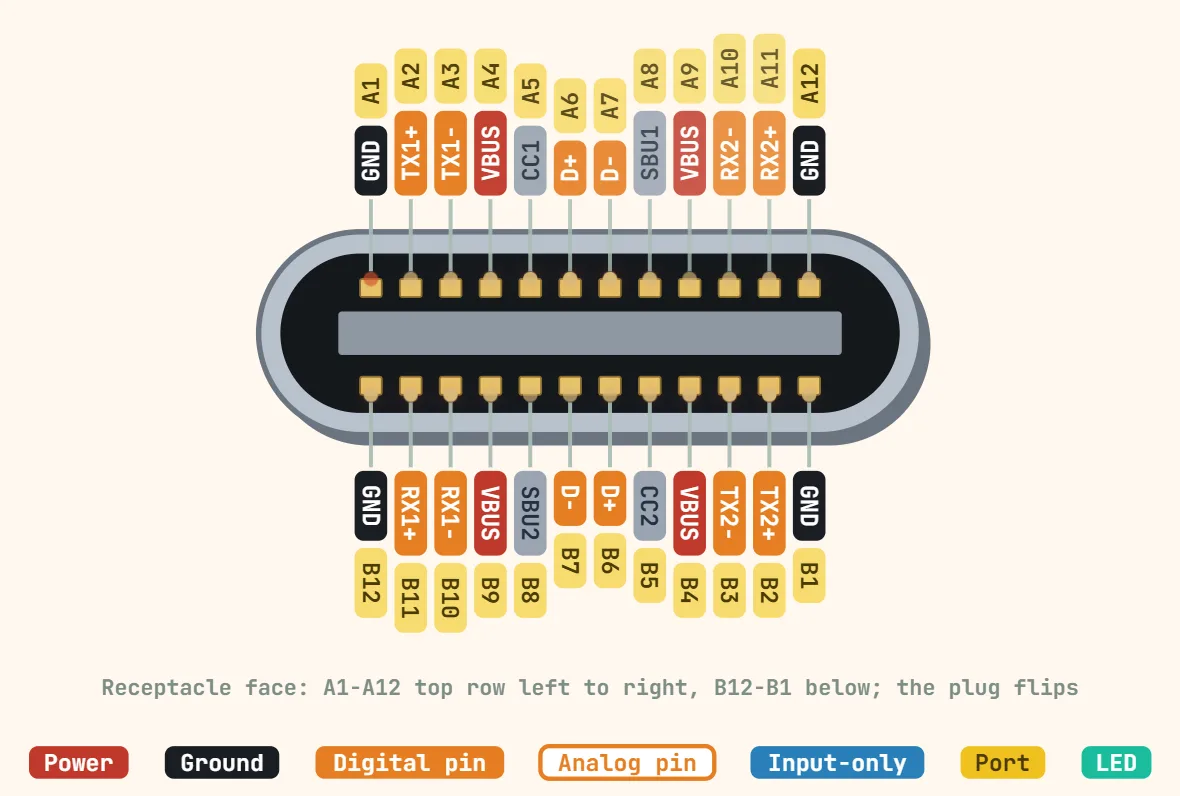
USB Type-C (USB-PD सक्षम रिसेप्टेकल) पिनआउट
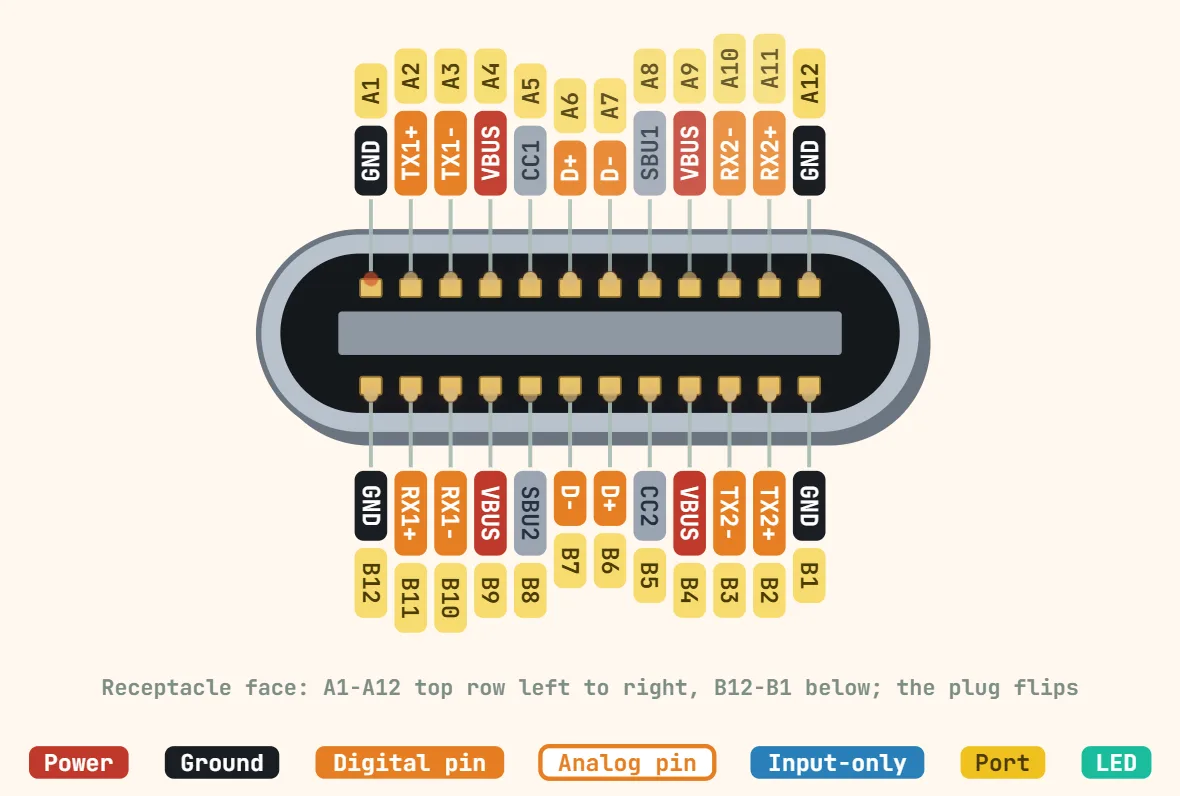
पिन
- A4/B4, A9/B9 — VBUS: four pins tied to one net, not four separate rails, so the current is split across more contact area; sits at a fixed 5V by default and only rises once a PD contract is actually negotiated over CC.
- A1/B1, A12/B12 — GND: the return path for VBUS and for both SuperSpeed pairs, likewise duplicated across four pins for current capacity, not wired as separate grounds.
- A5 — CC1, B5 — CC2: only whichever pin actually mates carries the Configuration Channel (the other is left floating or becomes VCONN — see below). Its DC level, set by an Rd/Rp resistor pair, is how the two ends first sense that something is even plugged in and which side is the power source, before any data moves.
- That same mated CC pin then carries the actual USB-PD protocol: Biphase Mark Coded (BMC) messages at a nominal 300 kb/s (±10%), built from a preamble, a message header, a data payload and a CRC — a real serial link, not a DC level, so a multimeter on CC only ever shows the idle Rp/Rd voltage and never the negotiation traffic.
- The CC pin that did NOT mate becomes VCONN whenever a cable needs it — an electronically-marked ("e-marked") cable, any USB 3.x/4 cable, or any link sourcing over 3A: the source or sink switches roughly 5V onto it, spec’d at a minimum of 1W (about 200mA) to run the cable’s ID chip and any signal redrivers inside it.
- A6/A7 and B6/B7 — two mirrored USB 2.0 D+/D− pairs; only one pair is actually driven per insertion, selected by which CC line mated. The second pair exists purely so the plug works either way up, not to add bandwidth.
- A2/A3+A10/A11 and B2/B3+B10/B11 — SSTX/SSRX SuperSpeed differential pairs (USB 3.x); same reasoning as D+/D−, only one full A-side or B-side set is live per orientation.
- A8/B8 — SBU1/SBU2: idle on plain USB and on PD itself, these are handed to an Alt Mode’s sideband channel (e.g. DisplayPort’s AUX line) once a Vendor-Defined Message negotiated over CC puts the port into that mode.
विनिर्देश
| कॉन्टैक्ट | 24 (रिसेप्टेकल) |
|---|---|
| डिफ़ॉल्ट VBUS | PD कॉन्ट्रैक्ट तय होने तक 5 V |
| PD तय वोल्टेज (SPR) | 5, 9, 15, 20 V |
| PD तय वोल्टेज (EPR, PD 3.1) | 28, 36, 48 V |
| अधिकतम करंट | 3 A; 5 A e-marked केबल के साथ 5 A |
| अधिकतम पावर | 100 W (SPR, 20 V × 5 A), 240 W (EPR, 48 V × 5 A) |
| PPS (PD 3.0) | 20 mV के स्टेप में 3.3–21 V |
| नेगोशिएशन | CC पर BMC, 300 kbit/s |
| VCONN | 5 V, कम से कम 1 W, e-marked केबल के लिए |
| सिंक ट्रिगर IC | STUSB4500, CH224, IP2721, FUSB302 |
नोट्स
- खाली USB-C कनेक्शन सिर्फ़ 5V की गारंटी देता है। हर ऊँचा "Standard Power Range" स्टेप (9V, 15V, 20V, और कुछ चार्जर पर 12V) और PD 3.1 में जोड़ा गया हर "Extended Power Range" स्टेप (28V, 36V, 48V, 5A/240W तक) ऐसा है जिसे सिंक को साफ़ तौर पर माँगना होता है और सोर्स को CC डेटा प्रोटोकॉल पर देना होता है — कोई रेज़िस्टर ट्रिक 9V+ नहीं देती, जैसे कुछ मालिकाना फ़ास्ट-चार्ज स्कीम असली PD के बिना कर लेती हैं।
- जो डिवाइस पीछे बिना किसी PD लॉजिक के सिर्फ़ तय 5.1 kΩ Rd से CC को नीचे खींचता है, उसे फिर भी पावर मिलती है (यह सादा "USB Type-C Current" है, सोर्स के चुने पुल-अप मान के अनुसार 5V/3A ≈15W तक सीमित) — लेकिन उसे 5V से ऊपर कभी कुछ नहीं मिलेगा, क्योंकि BMC हैंडशेक चलाने के लिए वहाँ कुछ नहीं है।
- अपना USB-PD स्टैक लिखे बिना PD चार्जर से 5V से ज़्यादा निकालने के लिए, एक समर्पित PD sink/trigger IC इस्तेमाल करें जो आपके लिए CC नेगोशिएशन चलाता है (जैसे STUSB4500, CH224, IP2721, FUSB302) और कॉन्ट्रैक्ट तय होने की सूचना देने के बाद तय वोल्टेज माँगने के लिए सरल पिन-स्ट्रैप या I2C इंटरफ़ेस देता है।
- सोर्स सिर्फ़ वही PDO देता है जो उसमें असल में हैं — एक बेसिक 5W/10W चार्जर 5V या 9V पर रुक सकता है, जबकि लैपटॉप चार्जर 20V तक, या नए EPR चार्जर पर 48V तक जा सकता है — इसलिए हर "PD चार्जर" को हर वोल्टेज तक पहुँचने वाला मानने के बजाय उसकी बताई Source_Capabilities जाँचें।
- VBUS और GND का चार-चार पिन पर फैला होना करंट क्षमता और कॉन्टैक्ट रेज़िस्टेंस का उपाय है, चार स्वतंत्र नेट नहीं — उदाहरण के लिए, A9 के VBUS को A4 वाले से अलग स्विच करने लायक न मानें।