مخطط الأطراف
مخطط أطراف ADC بـ 8 قنوات SPI من نوع MCP3008
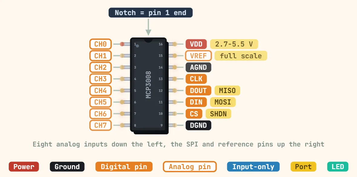
الأطراف
- 1: CH0 — analog input 0, one of eight single-ended channels (paired with CH1 as a differential pair when the SGL/DIFF config bit selects differential mode)
- 2: CH1 — analog input 1
- 3: CH2 — analog input 2
- 4: CH3 — analog input 3
- 5: CH4 — analog input 4
- 6: CH5 — analog input 5
- 7: CH6 — analog input 6
- 8: CH7 — analog input 7
- 9: DGND — digital ground, the return path for the SPI lines (CS, CLK, DIN, DOUT)
- 10: CS/SHDN — active-low chip select that also starts a conversion; taking it high deselects the chip and drops it into low-current standby (5nA typical, 2µA max per the datasheet, measured at CS = VDD = 5V)
- 11: DIN — SPI data in (MOSI); carries the start bit, the SGL/DIFF mode bit and the 3-bit channel address, latched on CLK's rising edge
- 12: DOUT — SPI data out (MISO); the 10-bit conversion result, shifted out MSB-first on CLK's falling edge
- 13: CLK — SPI serial clock, driven by the host; its safe maximum frequency depends on VDD (see notes)
- 14: AGND — analog ground, the reference return for the 8 input channels; tie to DGND at one point near the chip rather than routing them as two separate ground paths
- 15: VREF — external reference input that sets the full-scale (1023-count) reading; most designs tie it straight to VDD for a simple 0–VDD range, or to a precision reference chip when better accuracy than the supply rail is needed
- 16: VDD — positive supply, 2.7–5.5V; also sets the maximum usable SPI clock speed
المواصفات
| Resolution | 10-bit |
|---|---|
| Inputs | 8 single-ended or 4 pseudo-differential pairs |
| جهد التغذية | 2.7–5.5 V |
| Sample rate | 200 ksps at 5 V, 75 ksps at 2.7 V |
| الواجهة | SPI (modes 0,0 and 1,1) |
| أقصى ساعة SPI | 3.6 MHz at 5 V, 1.35 MHz at 2.7 V |
| Reference | External VREF, up to VDD |
| Linearity | ±1 LSB INL max |
| Supply current | 500 µA max active at 5 V; 2 µA max standby |
| Operating temperature | −40–85 °C |
| الغلاف | DIP-16, SOIC-16 |
الملاحظات
- VREF sets the full-scale reading (result ≈ Vin/VREF × 1023), and the datasheet's recommended operating condition is VREF ≤ VDD for a valid conversion — tying VREF to a noisy or sagging rail (or exceeding VDD) is a common source of readings that drift or clip well before the actual signal does.
- The maximum SPI clock scales with supply: the datasheet specifies about 3.6MHz at VDD=5V versus roughly 1.35MHz at VDD=2.7V, so on a Raspberry Pi's 3.3V rail (the usual pairing, since the Pi has no native ADC) most guides clock it conservatively — well under 1MHz is typical — rather than assuming the 5V-rated maximum applies.
- A conversion is a specific SPI bit sequence, not a plain byte read: a start bit, the SGL/DIFF bit and the 3-bit channel address go out on DIN first, then (after a sampling period and a null bit) the 10-bit result comes back on DOUT MSB-first; most drivers wrap this as three SPI bytes out/in with padding, so a hand-rolled bit-bang routine that gets the bit count or order wrong tends to return a plausible-looking but wrong number rather than an obvious error.
- CS/SHDN needs to go high between conversions (even briefly) to reset the chip's internal state machine before the next start bit — holding it permanently low, a habit carried over from always-selected I2C sensors, is a common reason a first attempt reads one stuck or garbled channel instead of cycling through CH0–CH7.