Diagrama de pines
Pines de Módulo ADC de 16 bits ADS1115 (I2C, breakout de 10 pines)
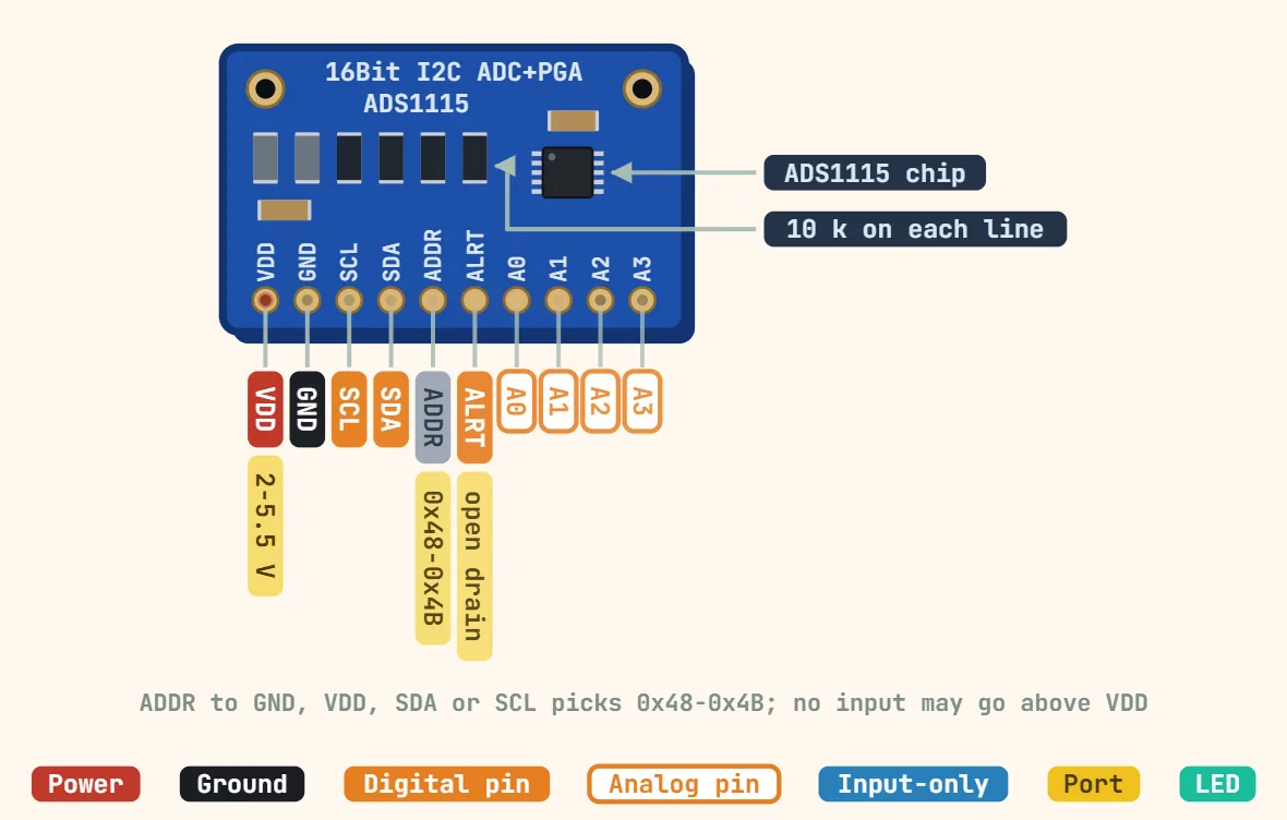
Pines
- VDD (2.0–5.5V — power it from the SAME rail as your MCU logic: the module fits 10kΩ pull-ups to VDD on SDA/SCL, so a 5V supply puts 5V on the I2C bus)
- GND (analog and digital ground — this is the reference for every single-ended reading, so it must be common with the circuit you are measuring)
- SCL (I2C clock — 400kHz fast mode, and up to 3.4MHz high-speed mode — already pulled up to VDD on the module, do not add another pull-up)
- SDA (I2C data — already pulled up to VDD on the module)
- ADDR (address select: tie to GND = 0x48, VDD = 0x49, SDA = 0x4A, SCL = 0x4B — the 10kΩ resistor above the pad normally pulls ADDR to GND, so an unconnected board answers at 0x48; wire it anyway if the address matters)
- ALRT / RDY (comparator alert or conversion-ready output, open-drain and active low — needs a pull-up to VDD; leave it unconnected if you poll instead)
- A0 (analog input 0 — must stay between GND−0.3V and VDD+0.3V whatever PGA range you pick: selecting ±6.144V does NOT make a 5V-powered board safe at 6V)
- A1 (analog input 1 — pairs with A0 as the A0−A1 differential channel)
- A2 (analog input 2)
- A3 (analog input 3 — pairs with A2 as the A2−A3 differential channel; 4 single-ended or 2 differential inputs, 8–860 SPS)
Especificaciones
| ADC IC | TI ADS1115 |
|---|---|
| Resolution | 16-bit |
| Sample rate | 8–860 samples/s, programmable |
| Inputs | 4 single-ended or 2 differential |
| Input ranges (PGA) | ±6.144, ±4.096, ±2.048, ±1.024, ±0.512, ±0.256 V |
| Tensión de alimentación | 2.0–5.5 V |
| Supply current | ≈ 150 µA typ in continuous mode |
| Interfaz | I2C, up to 400 kHz (3.4 MHz high-speed mode) |
| I2C address | 0x48 (ADDR to GND, default), 0x49 (VDD), 0x4A (SDA), 0x4B (SCL) |
| Extras | Internal reference and oscillator; programmable comparator on ALRT |
| Operating temperature | −40–125 °C |