Calculadora online gratuita
Timer NE555
Astável
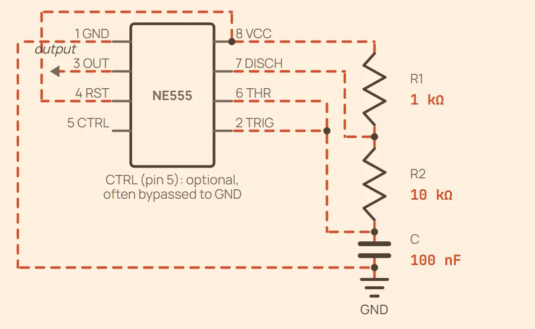
Rede de temporização totalmente ligada — os pinos estão agrupados por função, não pela ordem física do DIP (veja a entrada do temporizador 555 em Pinagens para a disposição real dos pinos). RST está ligado ao VCC para manter o chip habilitado; OUT é a saída de onda quadrada (vai para a carga que você estiver acionando); CTRL fica como indicado, já que é opcional para o funcionamento básico.
Exemplo Frequência: 685.7 Hz — ciclo de trabalho: 52.38 %
Ciclo de trabalho — informado abaixo como porcentagem. Ele nunca chega a 50 %: o capacitor carrega através de R1 + R2, mas descarrega só através de R2, então a fase alta é sempre a mais longa.
O que você informa
- R1 (Ω)
- R2 (Ω)
- C
Monoestável
Fully wired timing network — pins are grouped by function, not physical DIP order (see the 555 timer entry in Pinouts for the real pin layout). Pin 2 (TRIG) is not part of the R/C network — it needs a separate external trigger pulse. RST is tied to VCC to keep the chip enabled; OUT is the pulse output; CTRL is left as noted since it's optional for basic operation.
Exemplo Pulse width: 110 ms
One-shot pulse width: — the pulse starts when pin 2 (TRIG) is pulled below ⅓ Vcc.
O que você informa
- R (Ω)
- C
Biestável
Pins grouped by function, not physical DIP order (see the 555 timer entry in Pinouts for the real pin layout). Pulling SET below ⅓ Vcc latches OUT high; pulling RESET above ⅔ Vcc latches OUT low. DISCH (pin 7) is left unconnected — there's no timing capacitor to discharge in this mode. RST (pin 4) is tied to VCC to keep the chip enabled.
Exemplo No timing formula in this mode — OUT just follows whichever input (SET/RESET) was driven most recently. 10 kΩ is a typical pull resistor value; lower it if noise is falsely triggering an input.
No timing capacitor — SET (pin 2) and RESET (pin 6) are level-controlled inputs, each held to its resting state by a pull resistor until driven the other way.
O que você informa
- Pull-up R — SET (Ω)
- Pull-down R — RESET (Ω)