मुफ़्त ऑनलाइन कैलकुलेटर
NE555 टाइमर कैलकुलेटर
एस्टेबल
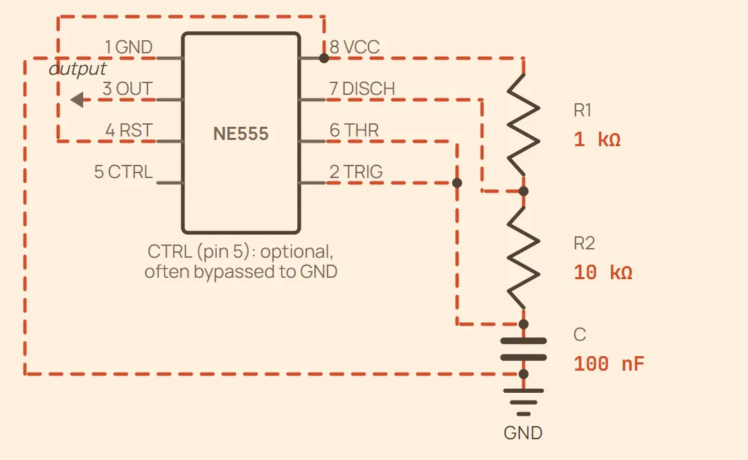
पूरी तरह जुड़ा टाइमिंग नेटवर्क — पिन फ़ंक्शन के अनुसार समूहित हैं, असली DIP क्रम में नहीं (असली पिन लेआउट के लिए Pinouts में 555 टाइमर देखें)। चिप चालू रखने के लिए RST को VCC से जोड़ा गया है; OUT स्क्वेयर-वेव आउटपुट है (जो भी लोड आप चला रहे हैं उसमें जाता है); CTRL को नोट के अनुसार छोड़ा गया है क्योंकि बेसिक काम के लिए यह वैकल्पिक है।
उदाहरण आवृत्ति: 685.7 Hz — ड्यूटी साइकल: 52.38 %
ड्यूटी साइकल — नीचे प्रतिशत में दिखाया गया है। यह कभी 50 % तक नहीं पहुँच सकता: कैपेसिटर R1 + R2 से चार्ज होता है लेकिन सिर्फ़ R2 से डिस्चार्ज होता है, इसलिए हाई फ़ेज़ हमेशा लंबा होता है।
आप क्या दर्ज करते हैं
- R1 (Ω)
- R2 (Ω)
- C
मोनोस्टेबल
Fully wired timing network — pins are grouped by function, not physical DIP order (see the 555 timer entry in Pinouts for the real pin layout). Pin 2 (TRIG) is not part of the R/C network — it needs a separate external trigger pulse. RST is tied to VCC to keep the chip enabled; OUT is the pulse output; CTRL is left as noted since it's optional for basic operation.
उदाहरण Pulse width: 110 ms
One-shot pulse width: — the pulse starts when pin 2 (TRIG) is pulled below ⅓ Vcc.
आप क्या दर्ज करते हैं
- R (Ω)
- C
बाइस्टेबल
Pins grouped by function, not physical DIP order (see the 555 timer entry in Pinouts for the real pin layout). Pulling SET below ⅓ Vcc latches OUT high; pulling RESET above ⅔ Vcc latches OUT low. DISCH (pin 7) is left unconnected — there's no timing capacitor to discharge in this mode. RST (pin 4) is tied to VCC to keep the chip enabled.
उदाहरण No timing formula in this mode — OUT just follows whichever input (SET/RESET) was driven most recently. 10 kΩ is a typical pull resistor value; lower it if noise is falsely triggering an input.
No timing capacitor — SET (pin 2) and RESET (pin 6) are level-controlled inputs, each held to its resting state by a pull resistor until driven the other way.
आप क्या दर्ज करते हैं
- Pull-up R — SET (Ω)
- Pull-down R — RESET (Ω)